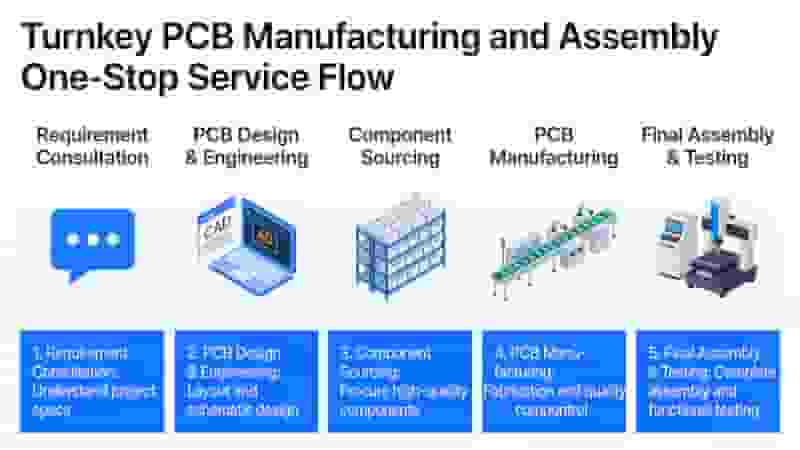
Turnkey PCB manufacturing and assembly provides a fully integrated end-to-end service covering design for manufacturing (DFM), bare board fabrication, electronic component sourcing, SMT assembly, THT assembly, functional testing, quality inspection and global shipping. This unified model reduces lead times, lowers total costs, improves quality consistency and simplifies project management for international electronics buyers, engineers and procurement teams.
What Is Turnkey PCB Manufacturing and Assembly
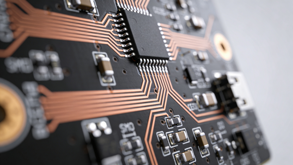
Turnkey PCB manufacturing and assembly is a complete one-stop service where one supplier manages the entire PCB production chain. We handle DFM analysis, bare PCB fabrication, components procurement, SMT/THT assembly, testing, quality control and global delivery in one integrated workflow.
This model eliminates coordination gaps between separate factories, reduces communication errors and ensures full process transparency for overseas buyers.
Core Advantages of One-Stop Turnkey PCB Solutions
1. Significant Cost Savings
We consolidate logistics, handling and management expenses into one streamlined process. Bulk component purchasing power reduces material costs, while fewer handoffs lower the risk of damage and rework.
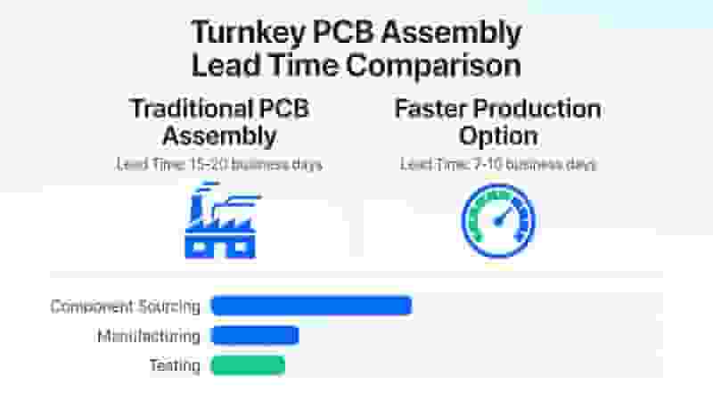
2. Shorter Lead Times & Faster Time-to-Market
With no delays from cross-vendor transfers or misalignment, turnkey PCB assembly cuts total lead times by 30–50% compared to traditional fragmented production.
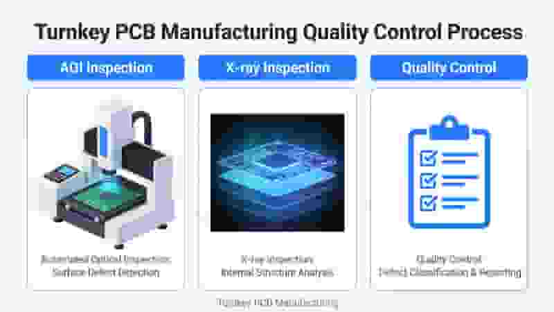
3. Higher Quality Control & Consistency
Unified quality standards run from design to finished PCBA. We implement IPC‑A‑610 standards, AOI, X‑ray inspection and functional testing to ensure reliability for industrial and commercial electronics.
4. Simplified Project Management
Overseas buyers enjoy a single point of contact for the entire project. This reduces communication complexity and speeds up problem resolution.
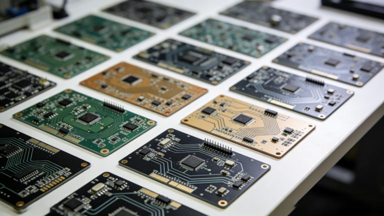
5. Strong Scalability & Flexibility
We support full project scaling from prototype PCB assembly to mass production, adapting to low‑volume high‑mix and high‑volume orders.
Standard Turnkey PCB Production Process
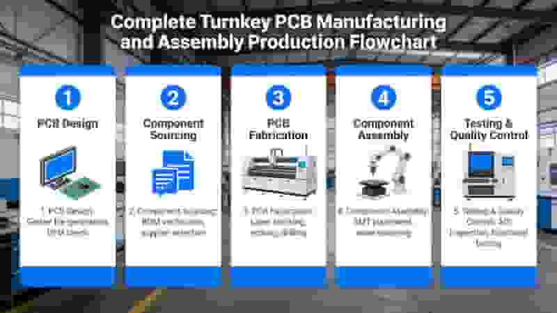
1. DFM/DFA Design Review
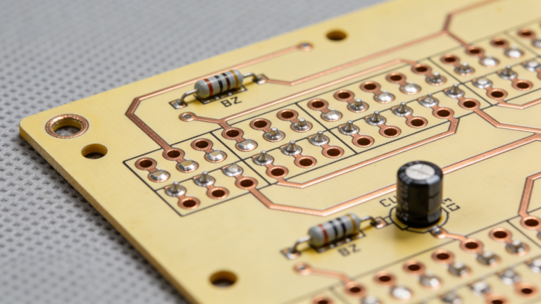
2. PCB Fabrication (inner layer → outer layer → solder mask → surface finish)
3. Electronic Components Sourcing
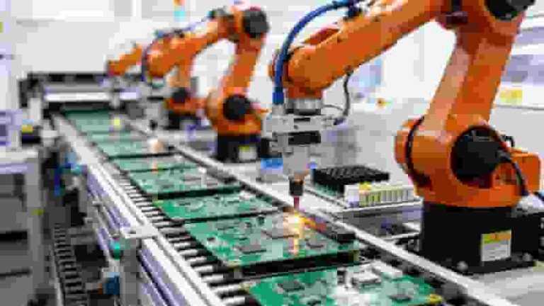
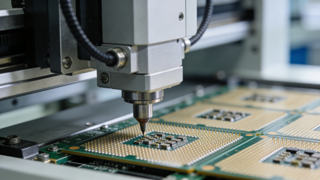
4. SMT Chip Mounting & Reflow Soldering
5. THT Through‑Hole Assembly
6. AOI, X‑ray & Functional Testing
7. Final Inspection & Packaging
8. Global Shipping & Logistics
Turnkey vs. Fragmented PCB Production Comparison
| Item | Turnkey PCB Solution | Fragmented Production |
|---|---|---|
| Lead Time | 30–50% faster | Longer, multiple handoffs |
| Total Cost | Lower overall cost | Higher hidden costs |
| Quality Consistency | Unified standard | Varies by vendor |
| Management Effort | Single point contact | Multiple vendors |
| Risk of Error | Very low | Higher |
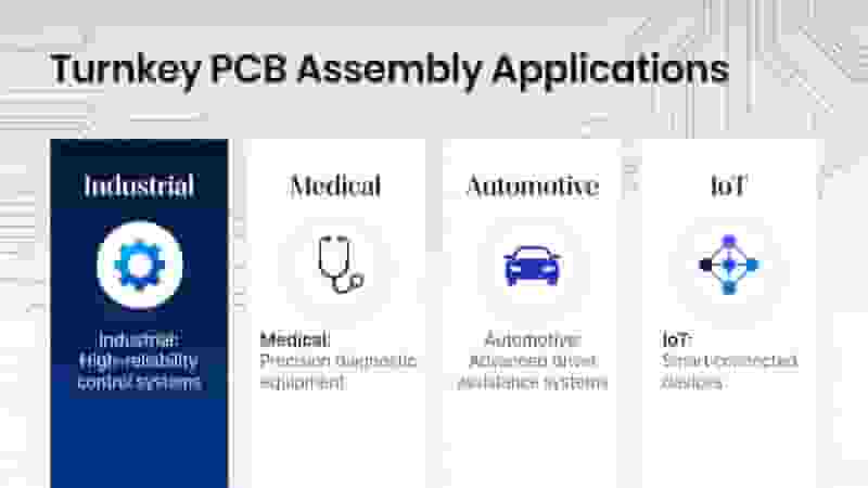
Key Industry Applications
Turnkey PCB manufacturing and assembly serves industrial automation, medical devices, automotive electronics, consumer electronics, IoT devices, communications equipment and aerospace applications.
How to Choose a Reliable Turnkey PCB Partner
– Certifications: ISO 9001, IPC, RoHS, REACH, UL
– Full in‑house capabilities: fabrication + assembly + testing
– Stable component supply chain
– Clear quality control process
– Strong global logistics and export experience
– Professional DFM support for overseas customers
Conclusion
Turnkey PCB manufacturing and assembly is the most efficient, cost‑effective and reliable solution for global electronics buyers seeking one‑stop PCB production. It reduces lead times, lowers costs, improves quality and simplifies international procurement.
By partnering with an experienced turnkey PCB supplier, you gain a stable, scalable and professional production chain to support your long‑term business growth.
Start Your Turnkey PCB Project Today
Get a free DFM review, custom quote and professional support for your turnkey PCB manufacturing and assembly needs.
Request a Free Quote
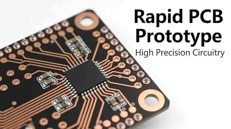
Accelerate Your Innovation with Rapid PCB Prototyping
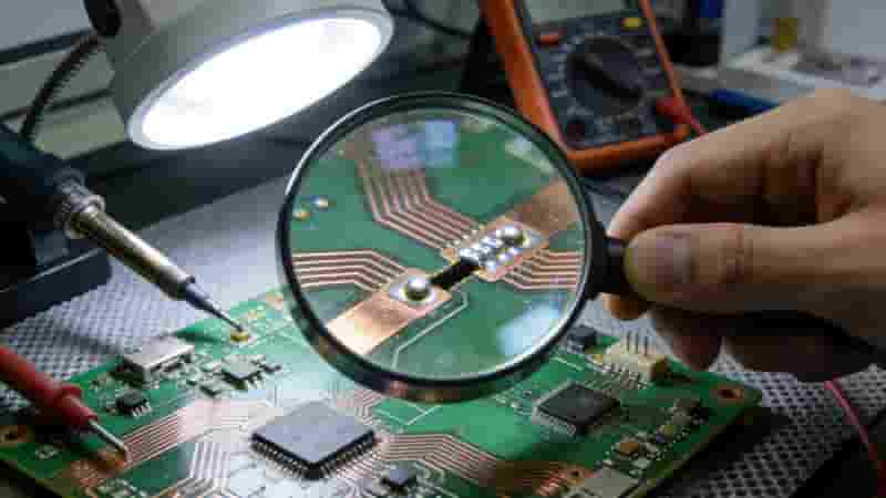
How to Test a PCB for Short Circuit: Complete Professional Guide
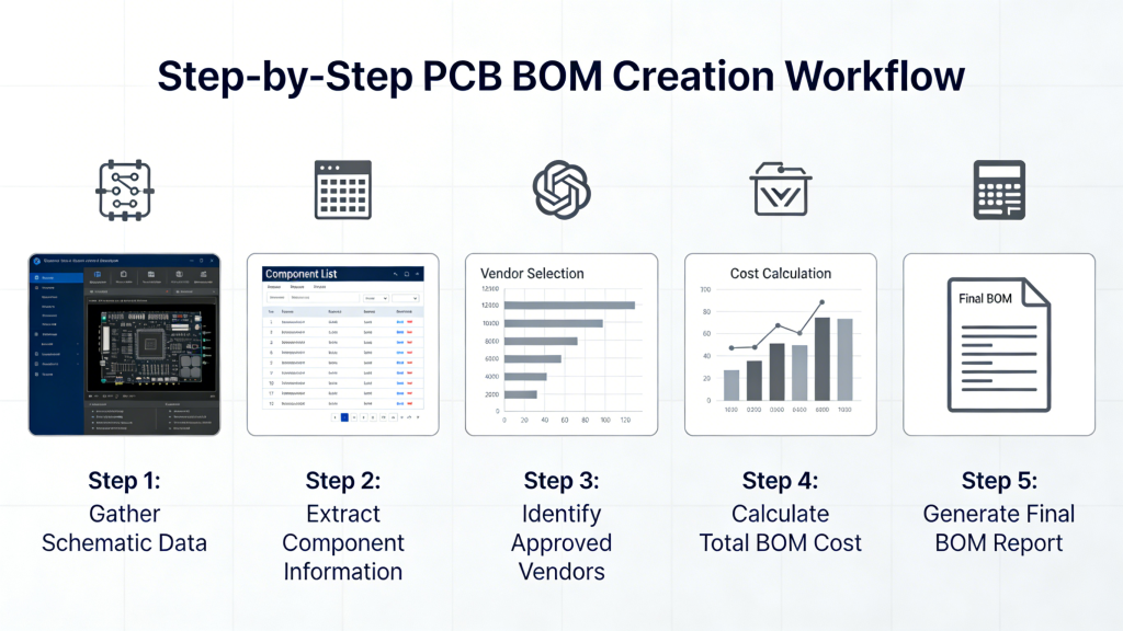
What is a PCB Bill of Materials (BOM) and How to Create One
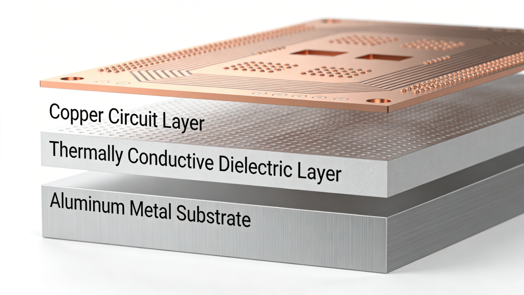
Professional Metal Core PCB (MCPCB) Manufacturing & Custom Service in China
Ball Grid Array (BGA) PCB Manufacturing & Assembly Services