|

Accelerate Your Innovation with Rapid PCB Prototyping

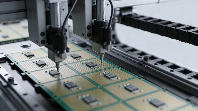
PCB prototyping process for design validation and testing

We provide professional Rapid PCB Prototyping with ultra‑fast lead times, strict quality control, and full customization for global engineers and buyers. From prototype to small‑batch production, we speed up your innovation and time‑to‑market.
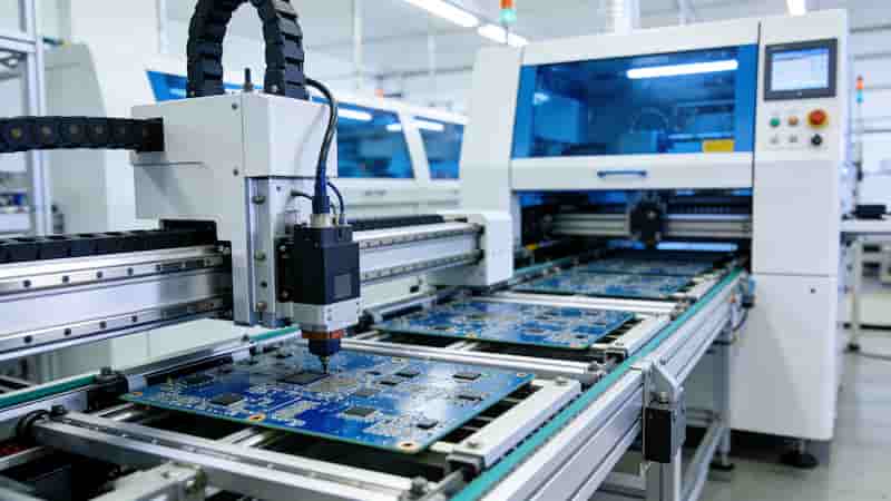
Rapid PCB Prototyping for fast product development and engineering validation

What Is Rapid PCB Prototyping

Rapid PCB Prototyping is the fast production of small‑batch printed circuit boards to validate design, function, and reliability before mass production. It helps engineers detect flaws early, optimize performance, and shorten product development cycles dramatically.

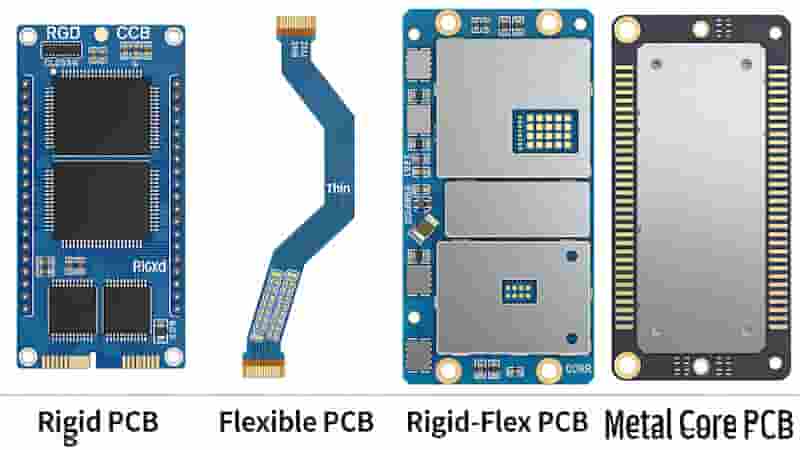
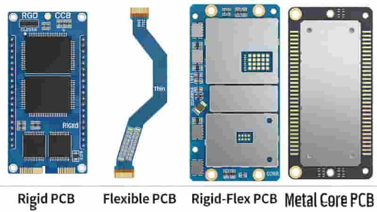
Our rapid PCB prototyping supports single‑sided, double‑sided, multilayer, rigid, flexible, and rigid‑flex boards to match modern electronic product demands.
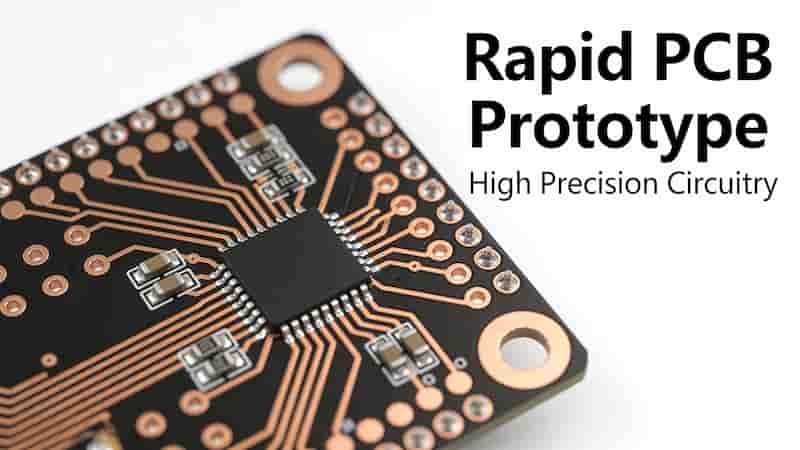
PCB prototyping process for design validation and testing

Why Choose Us for Rapid PCB Prototyping

We focus on speed, quality, and stability to support your innovation. Our advantages make us a reliable partner for global buyers:

  • Ultra‑fast turnaround: 8 hours for double‑sided prototypes, 24–72 hours for multilayer
  • Strict quality: IPC Class 2, RoHS, UL certified production
  • Low MOQ: 5–100 pieces for prototype testing and iteration
  • Full services: PCB fabrication + SMT assembly + component sourcing
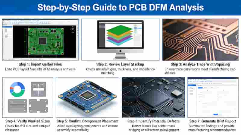
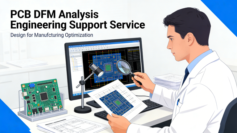
  • Free DFM review to optimize design and avoid production risks
  • Global delivery: DHL, FedEx, UPS for fast and safe shipping
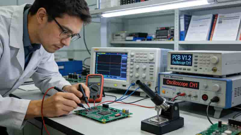
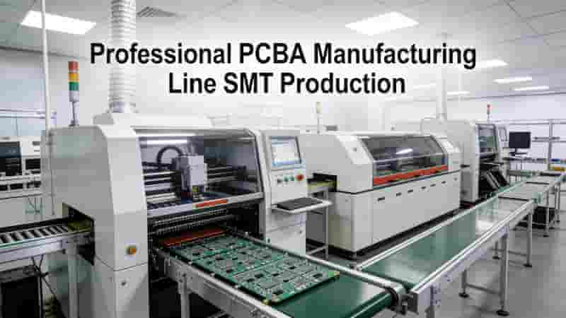
Professional rapid PCB prototyping manufacturing line

Key Benefits of Fast-Turn PCB Prototyping

Speed Up Time-to-Market
Fast rapid PCB prototyping cuts development cycles, helping you launch products ahead of competitors.

Ensure Stable & Reliable Design
Test and adjust early to eliminate hidden risks before mass production.

Reduce Overall Cost
Avoid expensive rework by validating designs in the prototype stage.

Support Complex Customization
We handle multilayer PCBs, blind vias, buried vias, flexible and rigid‑flex structures.

Rapid PCB Prototyping Lead Time Table

LayersWithin 0.1㎡0.1–1㎡1–2㎡
Single-layer24h / 48h24h / 48h3d / 5d
Double-layer8h / 24h24h / 48h3d / 7d
4 Layer2d / 3d3d / 4d4d / 8d
6 Layer3d / 4d4d / 5d5d / 10d
8 Layer3d / 4d4d / 5d6d / 11d

How to Get Rapid PCB Prototypes

1. Prepare your Gerber files and production requirements

2. Send files to get a free, fast quote

3. Confirm design and start rapid PCB prototyping

4. Full quality inspection before delivery

5. Fast global shipping to your address

Summary

Rapid PCB Prototyping is essential for modern product innovation. We deliver fast turnaround, high quality, full customization, and professional support to help engineers and buyers accelerate development, reduce risks, and launch products faster.

Start Your Rapid PCB Prototyping Now

Get free DFM check, fast quote, and high-quality rapid PCB prototyping in 8–72 hours.

Request a Free Quote
Contact for rapid PCB prototyping quote and custom service
HDI PCB Microvia Types: Blind, Buried, Stacked Vias

HDI PCB Layout and Basic HDI Design Guidelines

Posted on
0 Comments
HDI PCB is an advanced printed circuit board technology for high‑component‑density electronics. This guide covers core HDI PCB layout principles, via design, trace rules, stackup, and IPC standards for engineers and buyers. What Is HDI PCB Layout? High Density Interconnects (HDI PCB) layout refers to advanced PCB design techniques used when trace widths drop below…
PCB Order Process Flow for Prototyping Fabrication Assembly

How to Order PCB Prototyping, Fabrication & Assembly Services in China

Posted on
0 Comments
Get a clear quote within 24 hours and receive high-quality PCB prototypes in as fast as 3-5 days, with one-to-one engineering support from inquiry to delivery. Get a Free Quote Now 24h quotation · 3-5 day PCB prototyping · One-stop PCB & PCBA Why Engineers and Buyers Choose Us From fast PCB prototypes to full…
PCB Lead Time Comparison Prototype and Mass Production Volume

Key Differences Between Prototype and Production PCBs Explained

Posted on
0 Comments
Understanding prototype PCBs and production PCBs is essential for engineers, buyers, and project managers. This guide breaks down critical differences in lead time, cost, design flexibility, materials, testing, quality standards, and manufacturing processes to help you make informed decisions for your electronics projects. Introduction Printed circuit boards are foundational to nearly all electronic devices. The…
Buried PCB via connecting inner layers only

PCB Vias Explained: Through, Blind, and Buried Holes

Posted on
0 Comments
PCB vias connect layers in multilayer circuit boards, enabling compact, high-performance electronics. This guide covers plated through holes, blind, and buried vias, their design, manufacturing, and advantages in modern PCB fabrication. From 5G devices to automotive systems, understand how to choose the right via type for your project. What Are PCB Vias? A PCB via…
Copper Core PCB Structure - High Thermal Conductivity Copper Base

Copper Core PCB vs. Metal Core PCB: Key Differences & Advantages

Posted on
0 Comments
Copper Core PCB delivers superior thermal conductivity and stability for high-power electronics, while Metal Core PCB offers cost-effective thermal management for general industrial and commercial applications. Introduction to PCB Technology Printed Circuit Boards (PCBs) are the foundational building blocks of modern electronic devices. From consumer electronics to industrial machinery, PCBs ensure reliable electrical connectivity and…
Flying Probe Tester

SMT PCB Assembly Process: Step-by-Step Guide for High-Yield Production

Posted on
0 Comments
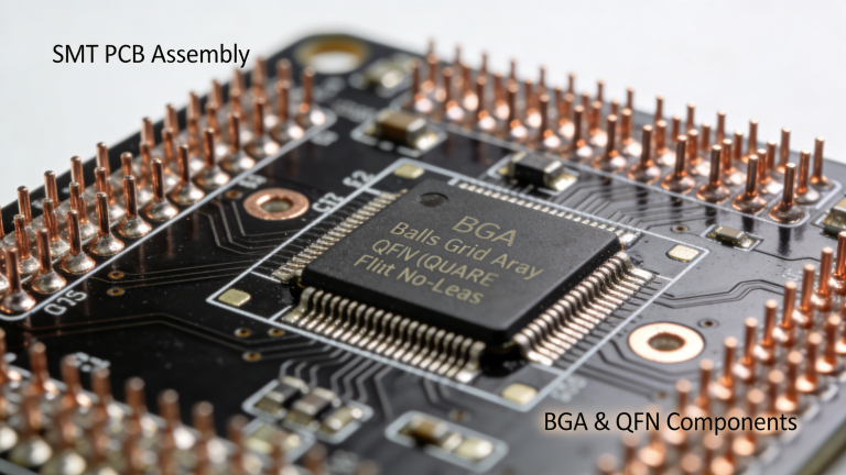
The SMT PCB assembly process is the core of modern electronics manufacturing. This guide walks you through each step, from barcode printing to final inspection, ensuring high reliability and efficiency for your PCBs. Introduction to SMT PCB Assembly Surface-mount technology (SMT) stands as the foundation of modern electronics manufacturing, supporting the production of compact, high-performance devices including…

FAQs About Rapid PCB Prototyping Service

A: Double-sided PCBs can be finished in 8 hours. Multilayer prototypes take 24 to 72 hours based on layer count and board size.

A: We support single-sided, double-sided, multilayer, rigid, flexible and rigid-flex PCBs, including designs with blind and buried vias.

A: MOQ starts from 5 pieces, suitable for prototype verification and multiple design iterations.

A: All products follow IPC Class 2, RoHS and UL requirements with complete quality control.

A: Yes. We provide PCB fabrication, component sourcing, SMT assembly and complimentary DFM review.

A: Please submit Gerber files and detailed production requirements to get a prompt quotation.

A: We use DHL, FedEx and UPS to deliver orders worldwide quickly and safely.

A: It shortens development cycles, removes potential risks, cuts post-production rework costs and supports complex customized designs.

Similar Posts