This guide gives a complete introduction to Copper Core PCBs, explaining their structure and unique advantages over standard FR4 and aluminum boards. Learn how copper core technology delivers superior thermal management, reliability, and electrical performance—making it ideal for high‑power, automotive, and industrial electronics. Explore types, design principles, manufacturing, FAQs, and how to select the right copper core PCB for your project.
What is a Copper Core PCB?
Copper Core PCB, sometimes called copper‑based PCB or copper substrate PCB, is a printed circuit board that uses copper as the main core material. Unlike traditional FR4 or aluminum PCBs, the copper core PCB provides outstanding thermal conductivity, mechanical strength, and electrical performance.
Copper is chosen for its fundamental properties: superior thermal management, mechanical stability, and excellent electrical conductivity. These traits make copper core PCB ideal for high‑power electronics, automotive systems, industrial controllers, and high‑performance LED products.
Key Features and Advantages of Copper Core PCBs
Copper Core PCBs solve critical engineering challenges in high‑performance electronics. Below are their core benefits:
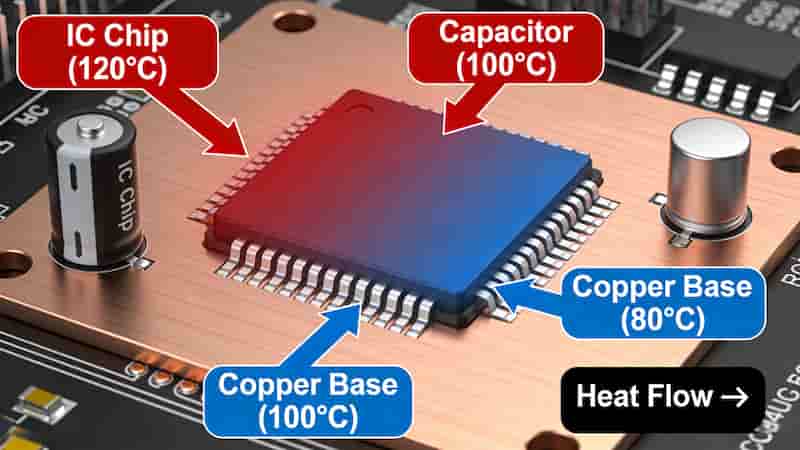
1. Outstanding Heat Dissipation
Copper’s high thermal conductivity rapidly transfers heat away from components, preventing overheating in LEDs, automotive power systems, and industrial machinery.
2. Superior Mechanical Strength
Copper cores add rigidity compared to FR4 or aluminum, reducing warpage during assembly and long‑term operation.
3. Enhanced Electrical Performance
Low electrical resistance lowers signal loss and supports higher current capacity for stable power delivery.
4. Durability and Reliability
Resistant to corrosion and extreme temperatures, suitable for harsh industrial and automotive environments.
5. Wide Application Versatility
Used in high‑power LEDs, automotive electronics, industrial controls, laser devices, medical, and aerospace systems.
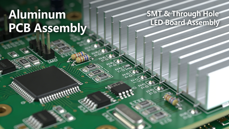
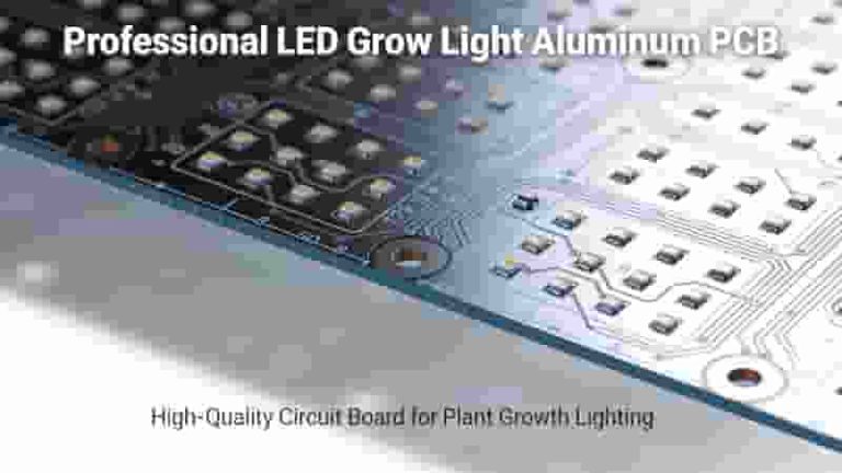
Real‑World Applications of Copper Core PCBs
Copper Core PCBs are widely used across industries requiring superior heat management and reliability:
LED Lighting Solutions
High‑power LEDs rely on copper core PCB for cooling, extending lifespan and maintaining brightness in commercial and automotive lighting.
Automotive Electronics
Used in engine controls, EV power systems, and safety electronics to resist thermal fatigue and ensure stable performance.
Industrial Equipment & Power Modules
Supports continuous high‑power operation in factory machinery and heavy‑duty control systems.
Laser, Medical & Aerospace Systems
Ensures uncompromising performance and safety in mission‑critical devices.
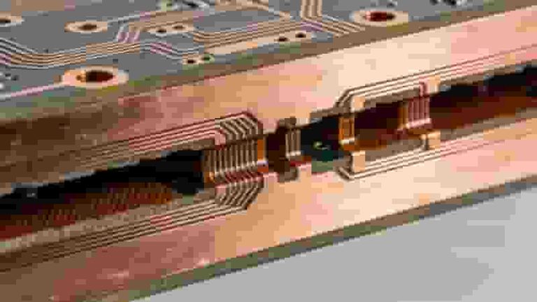
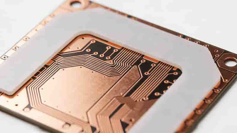
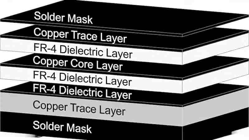
Structure and Types of Copper Core PCBs
Copper Core PCBs come in multiple designs to match technical requirements:
Single‑Layer Copper Core PCB
Basic structure for compact thermal management, ideal for small LED boards.
Double‑Layer & Multi‑Layer Copper Core PCBs
Supports high component density, complex routing, and greater power handling for industrial and automotive systems.
Copper Core Thickness
Range from 0.5mm to several millimeters, balancing heat dissipation and mechanical strength.
Copper Foil Thickness
Measured in oz/ft²; thicker foil improves current capacity for power applications.
Design and Manufacturing Process of Copper Core PCBs
High‑quality copper core PCB requires professional design and specialized manufacturing:
Design Considerations
Optimize heat flow, component placement, and trace width using Altium Designer or KiCad.
Material Selection
Choose core thickness, foil rating, and dielectric layers based on thermal and electrical needs.
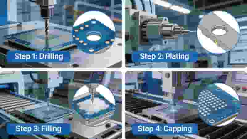
Manufacturing Steps
Substrate cutting → dielectric lamination → circuit etching → stack‑up bonding → surface treatment.
Surface Treatment
Anti‑oxidation layers or tin plating to enhance durability and solderability.
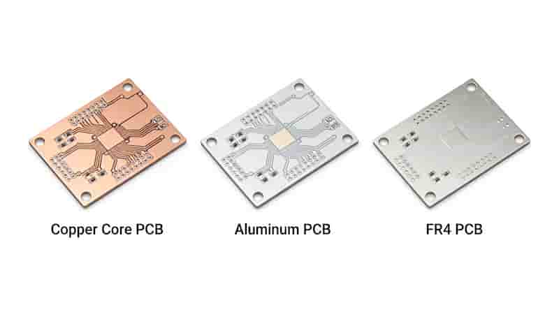
Copper Core PCB vs Aluminum PCB vs FR4 PCB
| Feature | Copper Core PCB | Aluminum PCB | FR4 PCB |
|---|---|---|---|
| Thermal Conductivity | Up to 400 W/mK | Up to 200 W/mK | Low |
| Mechanical Strength | Superior | Moderate | Standard |
| Best For | High‑power, critical use | Mid‑power, cost‑effective | General electronics |
Market Overview and Buying Guide
When sourcing copper core PCB, focus on these factors:
– Copper core thickness matching thermal requirements
– Copper foil specifications for current capacity
– Dimensional accuracy and tight tolerances
– ISO certifications and strict quality control
– Reliable lead time for prototyping and mass production
We provide customized copper core PCB solutions with full engineering support and international quality standards.
Conclusion & Future Trends
Copper Core PCBs are essential for high‑power, high‑reliability electronics. Growing demand in EVs, renewable energy, and smart industry will continue to drive adoption. With advanced thermal design and material innovation, copper core PCB remains a top choice for next‑generation electronic products.
Need a Custom Copper Core PCB Solution?
Contact us for free design review, official quotation, prototype service, and mass production support. We deliver reliable copper core PCB for global industrial and automotive clients.
Inquire Now | Get Free Quote
Step Stencils: Precision Solutions for Modern PCB Assembly
Fast Turnaround PCB Prototype Services from Certified Manufacturer
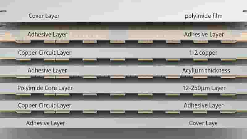
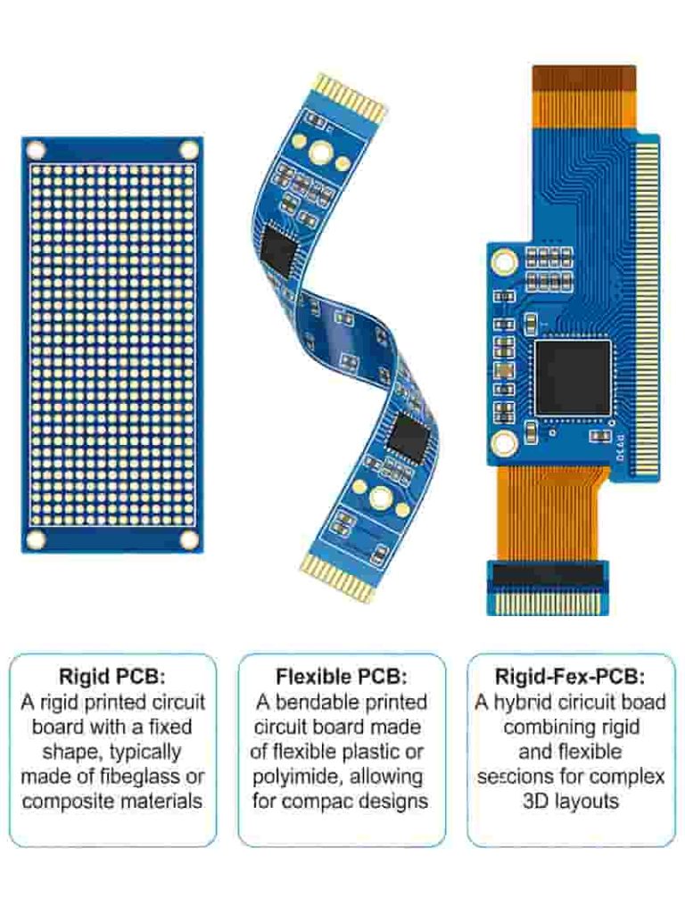
Types of Flexible Circuit Boards: The Ultimate Guide to Flex PCBs
PCB Manufacturing Capabilities

HDI PCB Manufacturing – Microvia, Blind & Buried Via HDI Boards up to 30 Layers