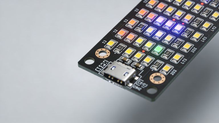
We provide professional HDI PCB manufacturing with laser‑drilled microvias, blind vias, buried vias, and advanced stack‑ups for high‑performance, compact electronic devices. Our services include fast prototyping, controlled impedance, strict quality control, and full DFM engineering support.
What Is an HDI PCB and Why Choose It?
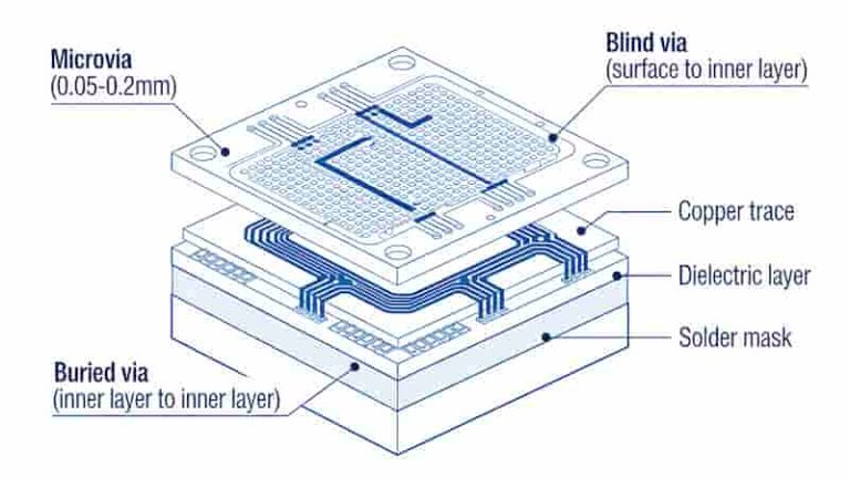
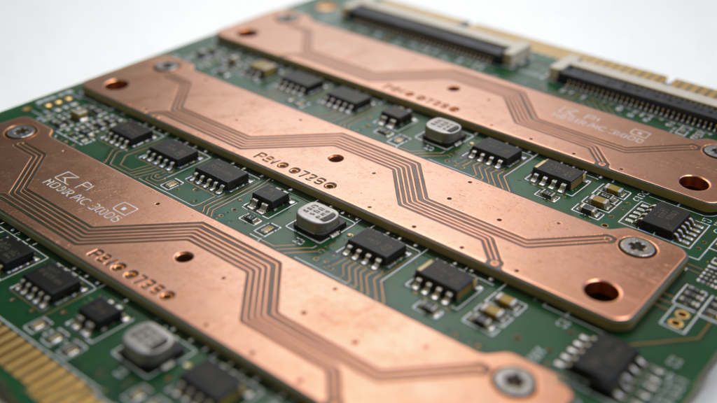
High‑density interconnect (HDI PCB) offers significantly higher wiring density than standard PCBs using microvias, blind and buried vias, fine lines, and thin‑core high‑performance materials.
By shortening signal paths, improving layer efficiency, and freeing routing space under fine‑pitch BGAs, HDI PCBs deliver smaller size, better signal integrity, higher reliability, and lower total system cost.
Key advantages of HDI PCB:
- Pack more functions into a smaller footprint with microvias and via‑in‑pad
- Improve signal integrity and reduce high‑speed noise
- Lower layer count and reduce overall BOM cost
- Enhance thermal performance and long‑term reliability
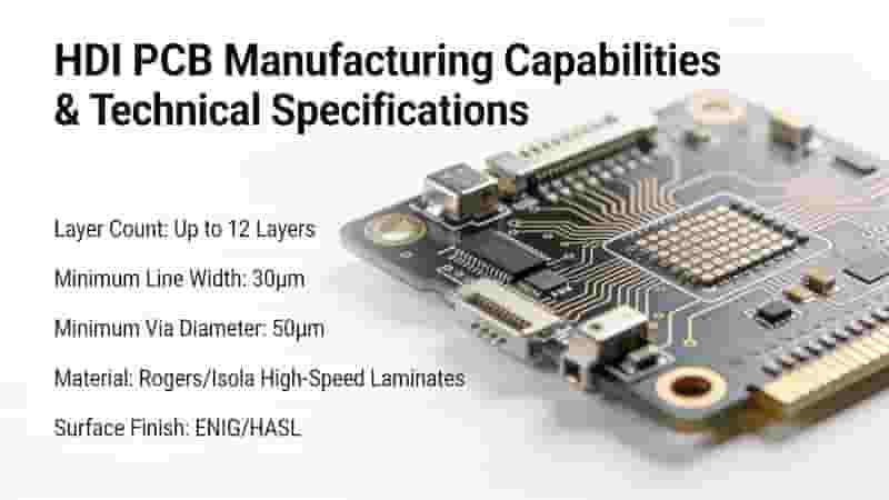
HDI PCB Manufacturing Capabilities
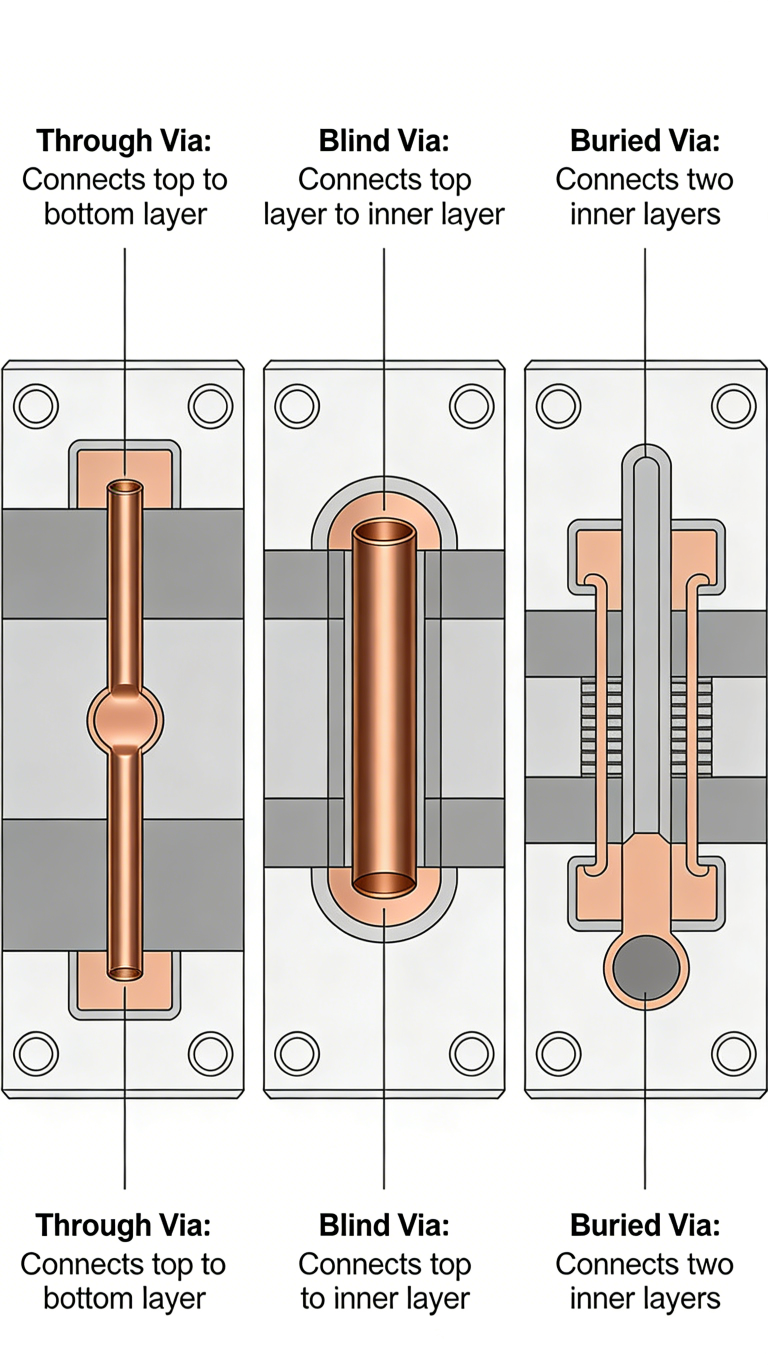
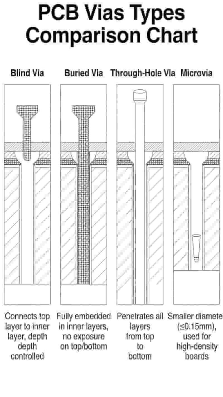
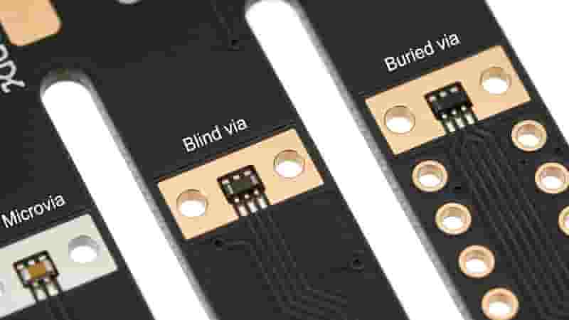
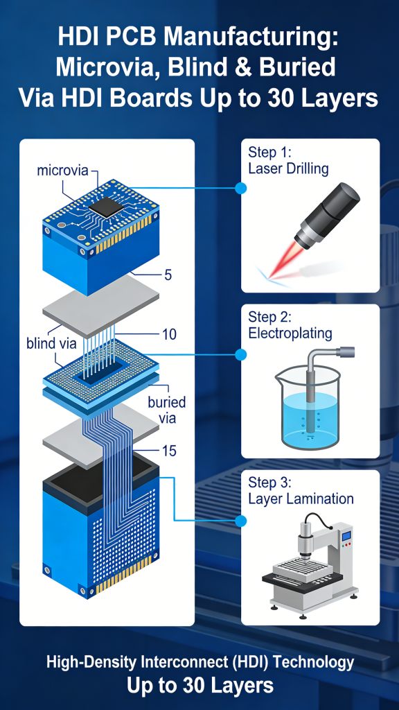
We specialize in HDI PCB fabrication supporting up to 30 layers, with laser microvias, blind/buried vias, stacked/staggered structures, and controlled impedance for industrial, automotive, 5G, and medical applications.
| Item | Specification |
|---|---|
| HDI Structure | 1+N+1, 2+N+2, 3+N+3, Any‑Layer (ELIC) |
| Max Layers | Up to 30 Layers |
| Min Trace/Space | 3/3 mil (0.075 mm) |
| Laser Microvia | 0.10 mm (4 mil), stacked / staggered |
| Materials | High‑Tg, low‑loss, halogen‑free laminates |
| Surface Finish | ENIG, ENEPIG, Immersion Ag/Sn, HASL, Gold Fingers |
| Certifications | UL, ISO 9001, IATF 16949, RoHS |
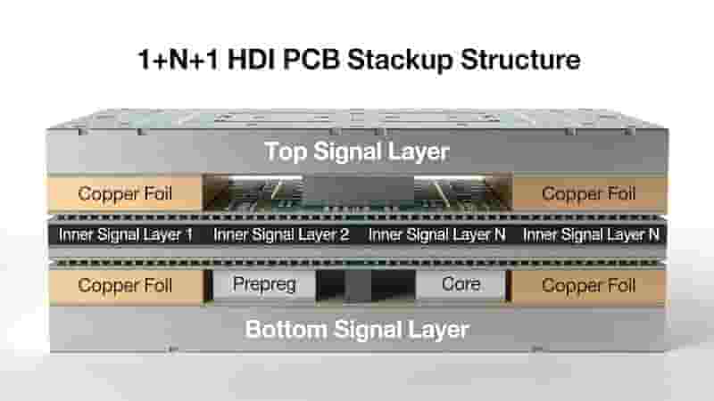
HDI Stackup Options for Different Designs
Selecting the right stackup balances HDI PCB density, performance, and cost.
1+N+1 HDI – Cost‑Effective Entry Level
Ideal for medium‑density designs, 0.5 mm BGA pitch, consumer electronics, IoT, and industrial controls.
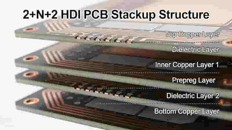
2+N+2 & 3+N+3 HDI – High Density
For fine‑pitch BGAs (≤0.4 mm), high‑speed signals, 5G, automotive, and high‑end computing.
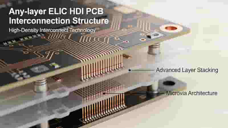
Any‑Layer (ELIC) HDI – Maximum Density
For ultra‑compact flagship devices, wearables, RF modules, and high‑speed computing.
Quality, Reliability & DFM Support
Our HDI PCB manufacturing uses strict process control and full inspection to ensure stability and longevity.
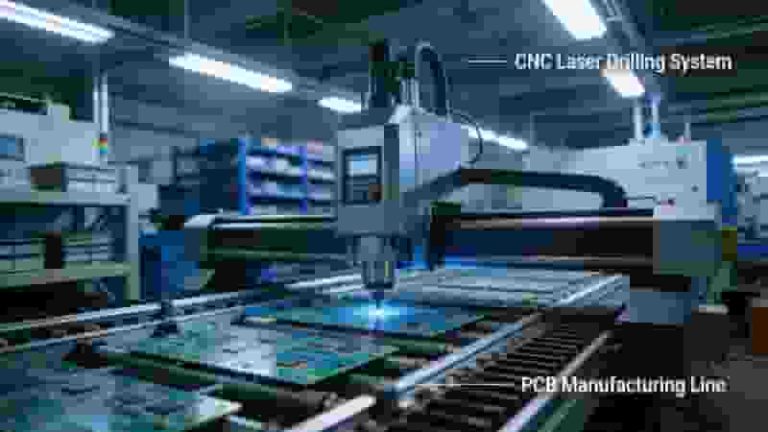
- Controlled laser drilling, sequential lamination, copper filling
- AOI, X‑ray, flying probe, and micro‑section analysis
- Professional HDI DFM review for yield and reliability
- Full material traceability and qualified laminate suppliers
HDI PCB Cost & Lead Time
Cost depends on stackup, layer count, microvias, materials, and tolerances. We help optimize design to reduce cost without sacrificing performance.
Typical Lead Time:
- Prototype: 5–8 working days
- Mass production: 10–15 working days
- Expedited rush service available upon request
No MOQ for HDI PCB prototypes; secure file upload and 24‑hour engineering review.
Applications & Industries We Serve
Our HDI PCB manufacturing supports global customers in high‑reliability fields:
- Automotive & EV: ADAS, ECU, infotainment, power control
- 5G & Telecom: high‑speed modules, routers, base stations
- Medical: portable devices, diagnostics, monitoring tools
- Consumer electronics & wearables: smartphones, tablets, IoT
- Industrial & IoT: automation, robotics, sensors
Summary
We are a professional HDI PCB manufacturing partner supporting up to 30 layers with microvias, blind/buried vias, controlled impedance, and full DFM support. Our UL, ISO, IATF 16949, and RoHS compliant processes ensure reliable quality for global industrial buyers, engineers, and procurement teams.
Request Your HDI PCB Quote Now
Upload your Gerber files and get a professional, fast quotation within 24 hours. No MOQ for prototypes.
Get HDI PCB Quote
PCB & PCBA Manufacturing Files: Complete Guide for Production & Quotation
Double-Sided Flex PCB Manufacturing Services | 2-Layer Flexible PCB Solutions
HDI PCB Manufacturing – Microvia, Blind & Buried Via HDI Boards up to 30 Layers
PCB Stackup Design Guidelines: Best Practices for 2, 4, 6 Layers
4 Layer PCB Manufacturing & Prototype Service | Factory Direct FR4 Stackup