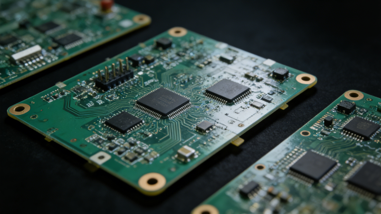
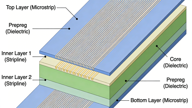
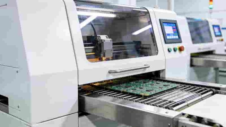
An aluminum PCB is a printed circuit board with a thin layer of conductive dielectric material—this special structure enables efficient heat dissipation, a key advantage over traditional PCBs. It is widely used in the LED lighting industry, especially for high-power LED fixtures like street lamps, downlights, and automotive headlights, where heat management directly affects product lifespan.
Here, we will detail the complete manufacturing process of aluminum PCBs, covering everything from raw material selection to final quality inspection. Whether you are a technical engineer seeking process details or a buyer wanting to understand production standards, you will find the professional and easy-to-understand information you need.
What is Aluminum PCB?
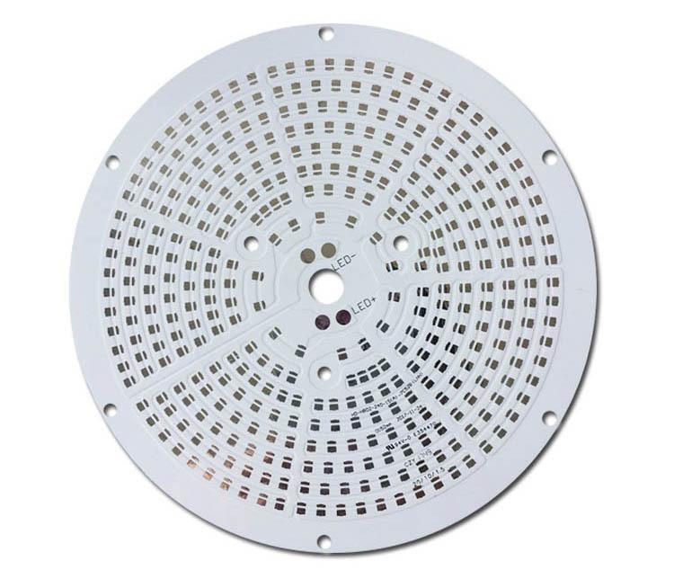
An aluminum PCB is a printed circuit board integrated with a thin layer of conductive dielectric material. This special structure gives it excellent thermal conductivity—one of its core advantages over traditional PCBs. It has multiple common names in the industry, including aluminum cladding, aluminum base, MCPCB (metal clad printed circuit board), IMS (insulated metal substrate), and thermal conductive PCB, which are often used interchangeably in technical communications.
First developed in the 1970s, aluminum PCBs quickly saw a surge in applications. Their initial use was in amplifying hybrid integrated circuits, where their heat-dissipating properties solved key performance issues of traditional boards. Today, they are widely used across industries like LED lighting, automotive electronics, and power supplies. Given their large-scale application in modern electronic products, understanding what aluminum PCBs are and their core value is essential for both technical practitioners and procurement professionals.
Aluminum PCB Manufacturing Process
We provide aluminum core PCBs with surface finish processes consistent with FR-4 PCBs, including Immersion Gold, Immersion Silver, and OSP. Below is the detailed manufacturing process of aluminum PCBs, categorized by surface finish types and internal operational steps.
1. Manufacturing Process by Surface Finish
1.1 Process for OSP Surface Finish
Cutting → Drilling → Circuit Fabrication → Acid/Alkaline Etching → Solder Mask Application → Silkscreen Printing → V-cut → PCB Functional Test → OSP Coating → FQC (Final Quality Control) → FQA (Final Quality Assurance) → Packaging → Delivery
1.2 Process for HASL Surface Finish
Cutting → Drilling → Circuit Fabrication → Acid/Alkaline Etching → Solder Mask Application → Silkscreen Printing → HASL (Hot Air Solder Leveling) → V-cut → PCB Functional Test → FQC → FQA → Packaging → Delivery
2. Detailed Internal Manufacturing Process of Aluminum PCB
Aluminum PCB Manufacturing Process Overview
| Step | Process Stage | Key Activity | Quality Control Focus |
|---|---|---|---|
| 1 | IQC | Incoming copper/aluminum inspection | Copper surface, protective film, thickness |
| 2 | Punching/Drilling | Positioning & technical holes | Hole position & diameter accuracy |
| 3 | Image Transfer | Film lamination, exposure, development | Alignment, photopolymerization, pattern formation |
| 4 | Image Inspection | Open/short circuit check | Gaps, incomplete development, black oil repair |
| 5 | Etching | Copper removal to form circuit | Protective film integrity, one-time thorough etching |
| 6 | Film Stripping | Remove dry film, clean board | Complete film removal, no residual solution |
| 7 | Etching Inspection | Final circuit pattern check | Short/gap/open circuits, mark defects |
| 8 | Solder Mask | Apply & expose solder mask | Surface cleanliness, alignment, protective film handling |
| 9 | Positioning Holes | Laminating punch for alignment | Hole position accuracy |
| 10 | Component Marks | Silkscreen printing | Clarity, no breaks or ghosting |
| 11 | HASL | Hot air solder leveling | Oven temperature, post-treatment cleaning |
| 12 | HASL Inspection | Tin surface quality check | Smoothness, coverage, color uniformity |
| 13 | Single-Sided Scrubbing | Clean aluminum surface (if required) | Brush type, trace width, protective film attachment |
| 14 | V-cut | Panel scoring for separation | Computer-aided, no adhesive peeling |
| 15 | Molding | Punch to final outline shape | No burrs, insulating layer integrity, tolerance |
| 16 | High-Pressure Test | Insulation strength verification | DC voltage, creepage current, operator safety |
| 17 | OSP Coating | Organic solderability preservative | Film thickness uniformity, aluminum surface color |
| 18 | FQC & FQA | Final quality control & assurance | Combined industry/customer standards, no pollution |
Step 1: IQC (Incoming Quality Control)
- Copper Surface Inspection: No notches, scratches, or severe oxidation are allowed.
- Protective Film Inspection: The protective film must be intact without exposing the copper layer.
- Thickness Inspection: Verify the board thickness and copper layer thickness according to the batch card specifications.
Step 2: One-Time Hole Punching/Drilling
- Purpose: Punch positioning holes and technical holes, ensuring hole position and diameter fully match the design drawing requirements.
- Operation Standard: Drill from the copper surface to the aluminum surface to effectively avoid scratches on the aluminum surface.
Step 3: Image Transfer
3.1 Surface Scrubbing
- Lightly scrub the protective film surface to enhance the adhesion between the dry film and protective film, preventing dry film peeling.
- The board surface must be free of oxidation and residual glue.
3.2 Film Lamination & Cooling
- Minimize the time interval between pre-curing and film lamination.
- After film lamination, let the aluminum board stand until it cools to room temperature to ensure accurate alignment during subsequent processes.
3.3 Exposure & Development
- Use negative yellow film, focusing on ensuring the alignment accuracy of silkscreen holes.
- The circuit area undergoes a photopolymerization reaction, which reaches full curing after 15 minutes.
- Perform development to form the preliminary circuit pattern.
Step 4: Image Inspection
- Focus on checking for open circuits, short circuits, gaps, and incomplete development.
- When repairing the board, use black oil instead of a black oil pen.
Step 5: Etching
- Mass production can only start after the first batch of boards is confirmed to be qualified.
- The protective film must be intact; if damaged, repair it with tape before placing the board in the etching machine.
- Ensure one-time thorough etching; do not use a knife to scrape residual copper on the pattern or dirt on the insulating layer.
Step 6: Film Stripping & Cleaning
- Use a roller to strip the film (instead of soaking in stripping solution) to ensure complete film removal.
- After stripping, thoroughly clean the board to remove residual stripping solution (residues will reduce the durability of the insulated metal substrate, IMS).
- Bake the board after stripping; manual etching is not allowed. If etching is incomplete, reprocess immediately.
Step 7: Etching Inspection
- Do not scratch any part of the insulating layer with a knife.
- Check for short circuits, gaps, and open circuits; mark unqualified units with an “X” using a black oil pen (do not drill holes in these units).
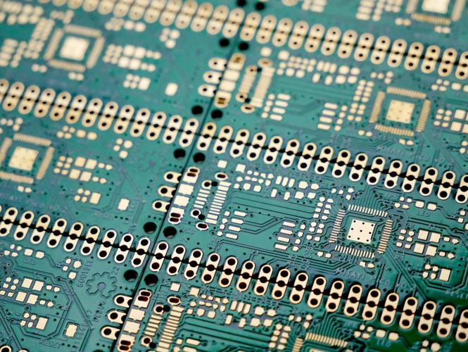
Step 8: Solder Mask Making
- Surface Preparation: Scrub the circuit side (single-sided scrubbing) to ensure no oxidation or glue residue on the board surface.
- Printing & Exposure: Print the solder mask only after the board cools to room temperature; align and expose the board after it cools again.
- Pre-Exposure Check: Before alignment, confirm there is no accumulation or uneven distribution of photosensitive oil on the board surface (reprocess immediately if issues are found).
- Post-Development Handling: For standard boards, remove the aluminum surface protective film after development (ensure no glue residue or film fragments remain). For custom boards with special requirements, keep the protective film intact throughout the production process.
- Reprocessing Note: Do not remove the protective film before reprocessing the solder mask; check for film damage and repair with tape if necessary.
Step 9: Positioning Hole Punching
- Use a laminating punch to create positioning holes at the specified positions on the board with completed circuits.
Step 10: Component Mark Making (Per MI Requirements)
- Conduct self-inspection for each printed board; only proceed to print the next board if the previous one is qualified. Separate and reprocess unqualified boards promptly.
- Component marks must be clear, with no breaks, ink seepage, or ghosting.
Step 11: HASL (Hot Air Solder Leveling)
- Control the tin oven temperature within the specified range.
- Perform post-treatment only after the board is fully cooled.
- Thoroughly clean the board surface in the hot water washing section of post-treatment to avoid dulling the board surface.
Step 12: HASL Inspection
- The tin surface must be smooth, with no tin buildup or uneven tin layers.
- Ensure all solder points are fully covered with tin.
- Mark points must be smooth; no protrusions or unevenness on the tin surface are allowed.
- The tin surface must have a uniform color and good luster, with no dull areas.
Step 13: Single-Sided Scrubbing (Per Customer Requirements)
- Clean the machine thoroughly and replace dirty water before scrubbing.
- Use felt rollers for scrubbing; select the specified brush types and ensure the scrubbing trace width is within the specified range.
- Clean the conveying rollers in the baking section before scrubbing.
- Use upper scrubbing brushes only; place the circuit side downward and turn off the lower scrubbing brushes.
- If there are scratches on the aluminum surface, smooth them with specified sandpaper before scrubbing.
- The tin surface must remain unpolluted and not dull; the aluminum surface must be scrubbed evenly.
- After confirming the aluminum and tin surfaces are qualified, attach a special colorless protective film to the aluminum surface.
Step 14: V-cut
- Use computer-aided V-cut equipment for processing.
- During V-cutting, do not tear off the adhesive paper or touch the aluminum surface with hands.
Step 15: Molding
- Throughout the process, do not tear off the adhesive paper or touch the aluminum surface with hands.
- Punch from the circuit side to the aluminum surface.
- The aluminum surface must have no obvious burrs; the board must not crack during punching, and the circuit side must remain unpolluted.
- The insulating layer must not peel off; the outline and positioning tolerance must meet design requirements.
- Clean the upper and lower molds during punching to remove metal shavings (shavings may damage the insulating layer and affect PCB electrical performance).
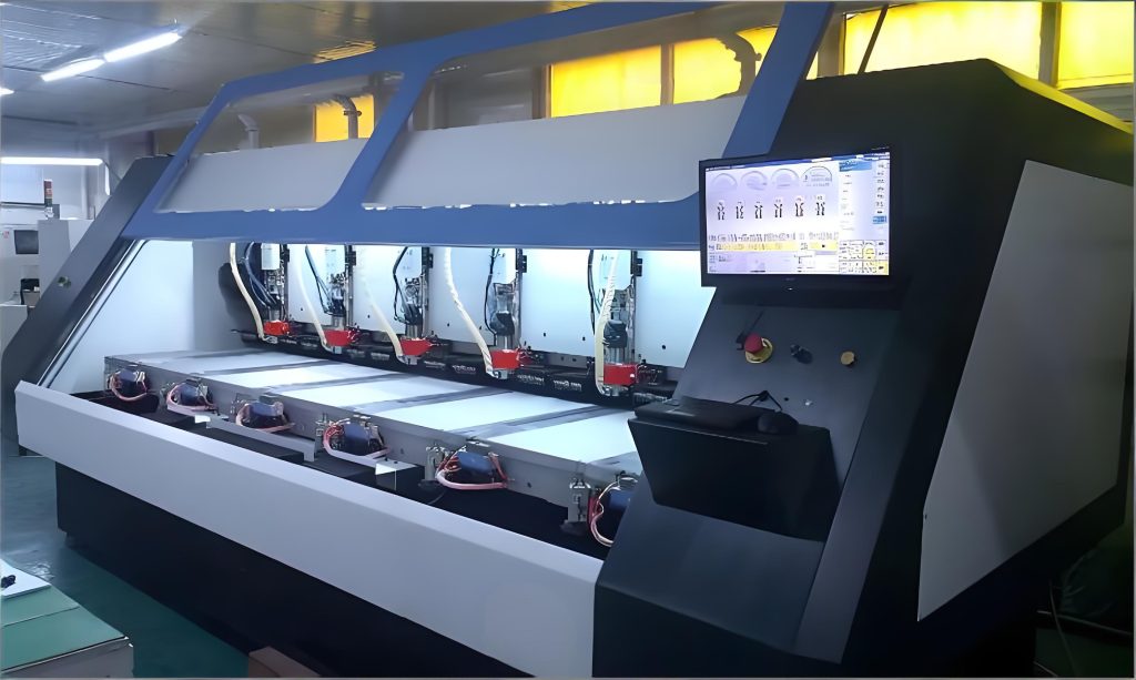
Step 16: High-Pressure Test
- Conduct the test according to customer requirements to ensure the aluminum PCB has sufficient insulation strength.
- Test parameters: DC voltage and creepage current per customer specifications.
- If creepage occurs during the test, test each board individually to identify defective units.
- Operators must wear insulated rubber shoes and gloves to avoid electric shock.
Step 17: OSP Coating
- The OSP film thickness must be within the specified range and evenly distributed.
- The aluminum surface color must remain unchanged, with no scratches.
Step 18: FQC & FQA Inspection
- Inspect the board based on a combination of aluminum PCB industry standards and customer-specific standards.
- Tear off the adhesive paper on the aluminum surface during inspection and separate boards with white paper.
- Ensure no pollution on the aluminum surface or circuit side during inspection.