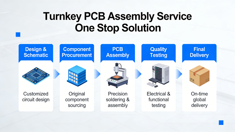
The SMT PCB assembly process is the core of modern electronics manufacturing. This guide walks you through each step, from barcode printing to final inspection, ensuring high reliability and efficiency for your PCBs.
Introduction to SMT PCB Assembly
Surface-mount technology (SMT) stands as the foundation of modern electronics manufacturing, supporting the production of compact, high-performance devices including smartphones, laptops, and IoT products. The SMT PCB assembly process integrates automation, precision, and efficiency to mount electronic components directly onto the surface of printed circuit boards (PCBs). Unlike traditional through-hole technology, SMT removes the need for drilling holes, enabling smaller, lighter, and more cost-effective designs. A typical SMT production line only requires 5–7 operators and can finish one PCB assembly in just 30–60 seconds, making it extremely suitable for high-volume production.
This guide offers a detailed breakdown of the entire SMT PCB assembly process, covering every stage from barcode printing to final inspection. Whether you are an electronics engineer, procurement specialist, or manufacturer, you will gain deep insights into technical details, best practices, and quality control procedures that ensure stable and reliable PCB assembly. By understanding these processes, you can optimize production efficiency, lower defect rates, and choose the most suitable SMT partner for your specific needs. Ready to explore SMT in detail? Let’s walk through the process step by step.
Key Features of SMT PCB Assembly Process
Surface-mount technology (SMT) refers to the process of mounting electronic components directly onto the surface of printed circuit boards (PCBs). By soldering components onto the PCB surface pads, SMT removes the need for drilling holes through the board, which is essential in traditional through-hole technology (THT). This method supports the production of smaller, lighter, and more sophisticated electronic devices, establishing SMT as the preferred solution for modern electronics manufacturing.
Key Advantages of SMT
- Miniaturization: SMT accommodates ultra-small components, enabling compact and sleek designs for smartphones, wearables, medical devices, and other advanced electronics.
- High Automation: SMT production lines utilize high-precision equipment including pick-and-place machines and reflow ovens, greatly reducing labor costs and minimizing human error.
- Enhanced Performance: Surface-mounted components feature shorter signal paths, which improve electrical performance, signal stability, and overall product reliability.
- Cost Efficiency: Automated assembly and higher component density help reduce overall production costs, especially in high-volume manufacturing scenarios.
SMT vs. THT: A Comparison
Unlike THT, which requires inserting component leads through pre-drilled holes and soldering on the reverse side, SMT attaches components directly onto the PCB surface. Although THT remains applicable for larger or high-power components, SMT has become the dominant technology thanks to its superior speed, precision, and compatibility with automated assembly. For instance, SMT systems can place thousands of components per hour, far exceeding the slower, labor-intensive THT process.
The versatility and efficiency of SMT make it essential across industries including consumer electronics, automotive, and aerospace. As technology continues to advance, SMT is constantly evolving to support even smaller components and increasingly complex PCB designs.
SMT PCB Assembly Process Steps
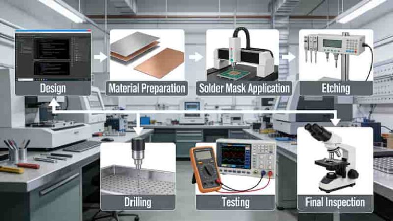
The SMT PCB assembly process is a highly automated workflow that converts bare printed circuit boards into fully functional electronic assemblies. Every stage, from initial preparation through final inspection, plays a critical role in guaranteeing quality, efficiency, and reliability. In this section, we start with the first step: Shop Floor Tracking through Barcode Printing.
Step 1: Shop Floor Tracking: Barcode Printing
Before assembly commences, a unique tracking barcode is printed on the bare PCB to enable real-time monitoring throughout the entire production flow. This barcode connects with the Shop Floor Control System (SFCS) or Shop Floor Data Collection System (SFDC), allowing manufacturers to track production progress, quality indicators, and potential defects.
There are three primary methods for applying barcodes:
- Label Paper: Adhesive labels with pre-printed barcodes, simple to apply but relatively low in durability.
- Inkjet Printing: Direct inkjet marking, offering high flexibility but requiring precise calibration to ensure readability.
- Laser Printing: Laser-etching barcodes directly onto the PCB surface, delivering excellent durability and precision.
Modern SMT production lines are increasingly adopting two-dimensional (2D) barcodes such as QR codes, which can store far more data in a smaller area than traditional one-dimensional barcodes.
Best Practices for Barcode Printing:
- Clarity and Scannability: Ensure barcodes are clear and scannable to prevent tracking errors.
- Durability: Choose a printing method that resists friction, high temperatures, and long-term storage without fading or damage.
- Positioning: Place barcodes in non-functional areas to avoid affecting the PCB’s performance or appearance.
Effective barcode implementation improves traceability, reduces quality issues, and optimizes production management, laying a solid foundation for a high-quality SMT assembly process.
Step 2: Bare Board Loading
The bare board loading stage marks the official entry of PCBs into the SMT production line. This critical step involves feeding blank, component-free boards onto the conveyor system for downstream assembly processes. Typically, bare boards are neatly stacked in material racks or magazines and automatically fed into the line one by one via mechanical equipment. This automated loading mechanism ensures accurate and efficient board handling, reducing downtime and sustaining stable production flow.
Two common bare board loading methods are widely used:
- Material Rack Loading:Boards are stacked and separated by a mechanical arm, which places them onto the conveyor. This approach is cost-efficient but carries a slight risk of surface scratches during handling.
- Magazine Loading:Boards are stored in protective magazines, greatly lowering the risk of physical damage. Magazines are engineered for smooth integration with SMT machinery, ensuring stable and consistent feeding.
Sensors monitor the entire loading process and transmit real-time data to the control system, which regulates board feeding and pausing to maximize production throughput. Proper loading prevents board misalignment and surface damage, which can negatively impact downstream processes such as solder paste printing.
Best Practices for Bare Board Loading:
- Use protective magazines for delicate or high-value PCBs to reduce scratches.
- Calibrate sensors regularly to ensure accurate positioning on the conveyor.
- Inspect racks and magazines for debris that may interfere with smooth loading.
By emphasizing precision and board protection, the bare board loading stage establishes a reliable foundation for a smooth SMT assembly process and consistent high-quality results.
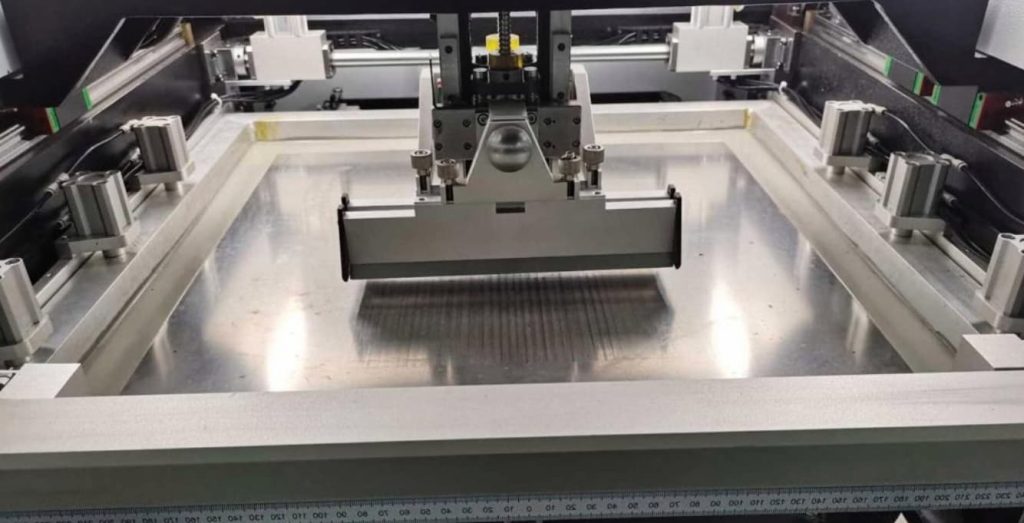
Step 3: Solder Paste Printing
Solder paste printing is a critical stage in the SMT PCB assembly process. During this step, solder paste—a mixture of fine solder particles and flux—is applied to the PCB pads. This paste performs two essential roles: it temporarily holds electronic components in place during placement, and creates permanent solder joints during reflow soldering. The paste is deposited through a precision SMT stencil, which aligns accurately with the PCB pads to ensure the right amount of paste is applied at the exact positions.
The quality of solder paste printing directly determines soldering reliability. Insufficient paste can result in weak or cold joints, while excessive paste may cause bridging and short circuits. Modern SMT production lines employ automated stencil printers with vision systems to guarantee precise alignment and consistent paste deposition.
Best Practices for Solder Paste Printing:
- Stencil Design: Use high-quality stainless steel stencils with laser-cut apertures that precisely match pad dimensions.
- Paste Control: Maintain proper solder paste viscosity and store it at the recommended temperature (usually 2–10°C) to avoid deterioration.
- Regular Maintenance: Clean stencils after every 5–10 prints to remove residue and prevent aperture clogging.
- Alignment Verification: Use vision systems to verify accurate stencil‑to‑PCB alignment before printing.
By optimizing solder paste printing, manufacturers can minimize defects and improve the reliability of the final PCB assembly, establishing a stable foundation for subsequent production steps.
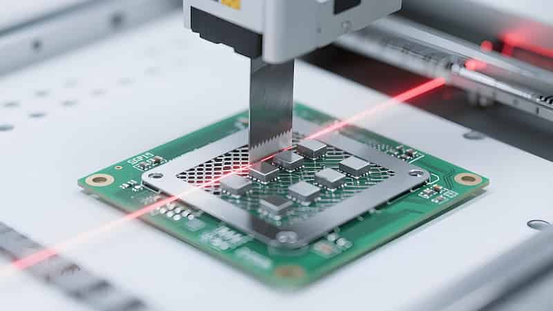
Step 4: Solder Paste Inspection (SPI)
Solder Paste Inspection (SPI) is a vital quality control step in the SMT PCB assembly process, conducted right after solder paste printing. SPI uses advanced optical equipment to inspect the quality of solder paste deposits on the PCB pads. By measuring key parameters including volume, height, area, and alignment, SPI identifies issues such as insufficient paste, excessive paste, or misalignment that may cause soldering defects like weak joints or short circuits.
The SPI system adopts 2D or 3D imaging technology, similar to Automated Optical Inspection (AOI), to scan the PCB surface. When defects are detected, the board can be cleaned and reprinted prior to component placement, greatly reducing rework expenses and scrap rates. Leading SMT manufacturers depend on SPI to maintain consistent soldering quality, particularly for high‑density and complex PCBs.
Best Practices for Solder Paste Inspection:
- Use 3D SPI Systems: 3D imaging delivers more precise measurements of paste volume and height than 2D systems.
- Set Strict Tolerances: Define acceptable paste parameters to detect defects early while minimizing false rejects.
- Regular Calibration: Calibrate SPI equipment routinely to ensure sustained accuracy and reliability.
- Act on Findings: Remove defective boards for cleaning or adjust printing settings to avoid repeated issues.
By detecting solder paste problems at an early stage, SPI improves the stability and reliability of the SMT assembly process, reduces defects, and ensures high‑quality solder joints.
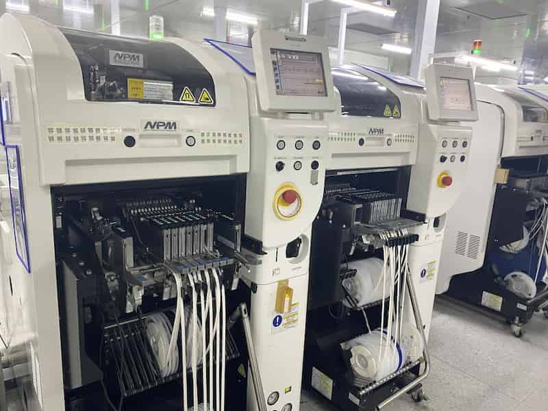
Step 5: High-Speed Chip Placement
High-speed chip placement is a core process in SMT PCB assembly, where miniature passive components—including resistors, capacitors, and inductors—are accurately positioned onto the solder paste‑coated pads of the PCB. Often known as “small chips,” these components typically feature only two terminals, demanding extremely high positional accuracy to guarantee reliable soldering. High-speed placement machines, fitted with multi‑nozzle heads, can place thousands of components per hour, making them highly suitable for mass production.
Equipped with precision vision systems and advanced software, the machine’s nozzles pick components from tape‑and‑reel feeders and place them onto the PCB. The tacky solder paste applied in the earlier step secures components in place during high‑speed board transfer, preventing misalignment. A standard SMT line often incorporates one to four high‑speed placement machines to maximize production throughput.
Best Practices for High-Speed Chip Placement:
- Calibrate Vision Systems: Regularly calibrate the machine’s cameras to ensure precise component alignment.
- Monitor Solder Paste Quality: Check the tackiness of solder paste to avoid component shifting during placement.
- Optimize Feeder Configuration: Arrange tape‑and‑reel feeders to reduce nozzle travel time and improve overall efficiency.
- Perform Regular Maintenance: Clean nozzles and inspect for wear to prevent pickup failures or placement defects.
High-speed chip placement significantly boosts production efficiency while maintaining strict precision, laying the groundwork for the subsequent stages in the SMT assembly process.
Step 6: General Pick and Place
General pick and place, often called “precision placement,” is a key stage in the SMT PCB assembly process. It handles larger, heavier, or multi‑pin components such as Ball Grid Arrays (BGAs), connectors, card readers, and shielding cans. Unlike high‑speed placement machines that prioritize speed for miniature passive components, general pick and place machines focus on high precision and flexibility. Equipped with advanced vision systems, these machines capture component images, adjust position and angle, and accurately place components onto the solder paste‑coated pads of the PCB.
Components used in this stage often come in alternative packaging formats such as trays or tubes, instead of standard tape‑and‑reel. Some irregularly shaped components may need custom nozzles or flat tape to ensure proper suction by the machine’s nozzles. The relatively lower placement speed guarantees precise alignment, which is essential for complex components with numerous pins or strict tolerances.
Best Practices for General Pick and Place:
- Use Vision‑Guided Alignment: Calibrate cameras regularly to ensure accurate positioning and angle correction for multi‑pin devices.
- Customize Nozzles: Apply specialized nozzles for non‑standard components to ensure stable pickup and placement.
- Check Component Packaging: Confirm that trays or tubes are machine‑compatible to avoid feeding errors.
- Monitor Placement Accuracy: Inspect placed components routinely to prevent misalignment or offset issues.
By emphasizing precision, general pick and place ensures reliable mounting of complex components, improving the overall quality and reliability of the SMT assembly process.
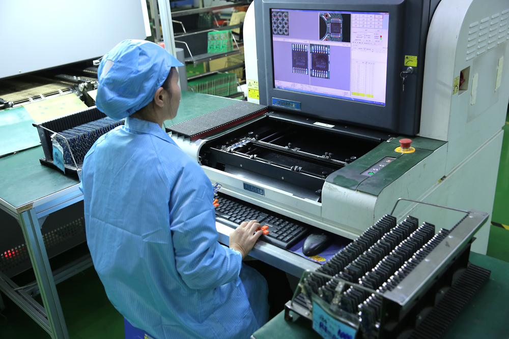
Step 7: Pre-Reflow Inspection, Visual or AOI
Pre-reflow inspection is an essential quality control step in the SMT PCB assembly process, performed after component placement and prior to reflow soldering. This stage verifies that components are accurately positioned and free from defects such as misalignment, missing parts, or reversed polarity. Inspection can be carried out either manually (visual inspection) or via Automated Optical Inspection (AOI) systems, which use high-resolution cameras to scan the PCB surface and identify anomalies with high precision.
AOI is especially effective for high-density PCBs, as it rapidly detects issues that could result in soldering defects, minimizing expensive rework after reflow soldering. However, some components such as shielding cans may block the AOI’s view, requiring additional visual inspection. For assemblies that involve manual placement of large or through‑hole components, this step also provides an opportunity to install these parts before soldering.
Best Practices for Pre‑Reflow Inspection:
- Combine AOI and Visual Checks: Use AOI for speed and accuracy, supplemented by manual inspection for areas blocked from optical detection.
- Calibrate AOI Systems: Regularly calibrate cameras and software to reduce false positives and reliably detect subtle defects.
- Train Inspectors: Provide visual inspectors with reference templates or guidelines to ensure consistent and accurate checks.
- Address Obstructions: Adjust PCB layout or inspection procedures to accommodate components like shielding cans that limit AOI visibility.
Effective pre-reflow inspection improves soldering quality and lowers post‑reflow rework rates, supporting a stable and reliable SMT assembly process.
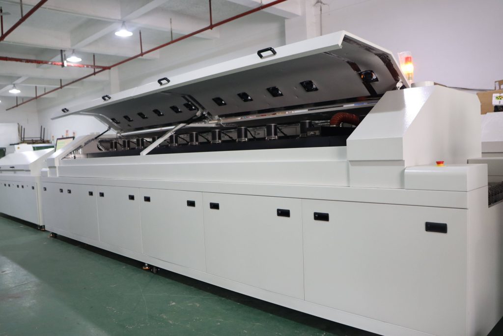
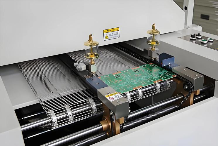
Step 8: Reflow Soldering
Reflow soldering is a critical stage in the SMT PCB assembly process, during which solder paste melts to form strong, permanent connections between electronic components and the PCB. This process takes place in a reflow oven, which exposes the PCB to a precisely controlled temperature profile with four key zones: pre-heat, soak, reflow, and cooling. The pre-heat zone gradually increases the board temperature, the soak zone activates the flux within the solder paste, the reflow zone melts the paste to form intermetallic compounds (IMCs), and the cooling zone solidifies the solder joints.
For lead-free solder pastes such as SAC305, the reflow oven must reach a minimum temperature of 217°C to melt the paste, while temperatures should not exceed 250°C to prevent damage to heat-sensitive components. Accurate temperature control is essential to avoid common defects including tombstoning, solder bridging, and component distortion.
Best Practices for Reflow Soldering:
- Optimize Temperature Profile: Adjust the pre-heat, soak, reflow, and cooling zones according to the specifications of the solder paste, such as the 217°C melting point of SAC305.
- Monitor Oven Conditions: Regularly calibrate the reflow oven to maintain stable temperatures and eliminate hot spots.
- Use Nitrogen Atmosphere: For high-reliability PCBs, a nitrogen environment reduces oxidation and enhances the quality of solder joints.
- Perform Post-Reflow Inspection: Check for defects such as voids or insufficient joints immediately after cooling to resolve issues at an early stage.
Effective reflow soldering guarantees robust, high-quality solder joints and completes the core assembly of the PCB.
Step 9: Post-Reflow AOI
Post-reflow Automated Optical Inspection (AOI) is a critical quality assurance step in the SMT PCB assembly process, carried out after reflow soldering to assess the quality of solder joints and component placement. Equipped with high‑resolution cameras and advanced software, AOI systems scan the PCB to identify defects including tombstoning, solder bridging, missing components, misalignment, and reversed polarity. This inspection is particularly vital for high‑density PCBs, where manual inspection is often impractical due to miniature component size and high complexity.
While AOI delivers high efficiency, it also has inherent limitations. It cannot inspect solder joints hidden under components such as Ball Grid Arrays (BGAs), nor can it detect issues like cold joints or actual component functionality. Shadowing caused by tall components may also reduce detection accuracy. For this reason, AOI is often combined with In‑Circuit Testing (ICT) or Functional Verification Testing (FVT) to achieve complete and reliable quality control.
Best Practices for Post‑Reflow AOI:
- Optimize Lighting and Angles: Adjust AOI camera and lighting settings to reduce shadow interference and improve defect detection.
- Integrate Complementary Tests: Use AOI together with ICT or FVT to cover blind spots such as hidden solder joints.
- Update Software Regularly: Keep AOI algorithms updated to minimize false positives and improve inspection accuracy.
- Focus on Critical Components: Pay close attention to high‑risk devices such as QFNs and connectors to ensure stable performance.
Post-reflow AOI strengthens quality control, detects defects early, reduces rework, and ensures the reliability of finished PCB assemblies.
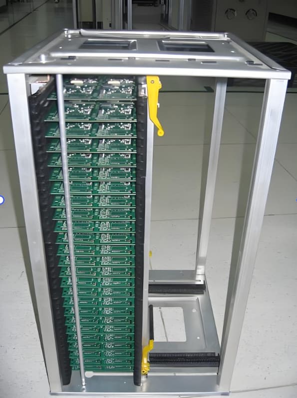
Step 10: Unloading
Unloading marks the final stage of the core SMT PCB assembly process, where fully assembled boards are removed from the production line and placed into protective magazines for storage or further processing. After completing reflow soldering and post‑reflow inspections, the PCBs are conveyed to an automated unloading system. These systems use mechanical arms or vacuum grippers to carefully transfer the boards into magazines, preventing damage to delicate solder joints and components.
Magazines are designed to safely hold multiple PCBs, shielding them from physical stress, dust, static discharge, and other environmental risks. In modern SMT lines, the unloading process is fully automated, with sensors ensuring accurate placement and reducing handling errors. Proper unloading is essential to preserve PCB quality before visual inspection or additional testing.
Best Practices for Unloading:
- Use Compatible Magazines: Select magazines that match PCB dimensions and SMT equipment requirements to avoid misalignment or damage.
- Minimize Manual Handling: Rely on automation to reduce human contact and maintain solder joint integrity.
- Control Environmental Conditions: Regulate humidity and static levels to protect sensitive electronic components.
- Inspect Magazines Regularly: Clean and check magazines for debris or wear to prevent scratches or contamination.
Effective unloading ensures assembled PCBs remain intact and ready for subsequent quality control or packaging, bringing a reliable conclusion to the SMT assembly process.
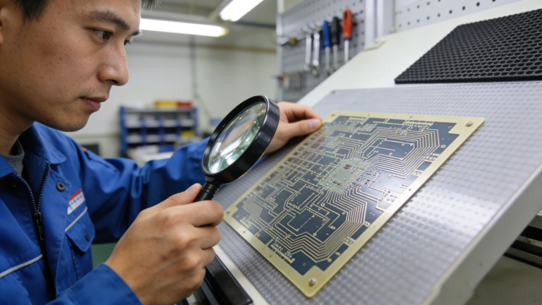
Step 11: Visual Inspection
Visual inspection is a key quality control procedure in the SMT PCB assembly process, usually carried out after unloading to verify the quality of finished assembled boards. This manual inspection serves as a valuable complement to Automated Optical Inspection (AOI), addressing defects that AOI may fail to detect—such as subtle solder joint flaws, component polarity errors, or issues in areas blocked by components like shielding cans. Trained inspectors use magnification tools and standardized templates to maintain consistency and accuracy.
While AOI is effective at identifying obvious defects including tombstoning and misalignment, visual inspection remains critical for high‑reliability PCBs, where human judgment can recognize subtle details overlooked by automated systems. For instance, inspectors can assess solder joint uniformity and confirm the orientation of critical components. This step lowers the risk of defective boards reaching end‑users and improves overall product reliability.
Best Practices for Visual Inspection:
- Use Inspection Templates: Provide clear guidelines or templates to standardize checks for solder quality and component positioning.
- Provide Comprehensive Training: Ensure inspectors are proficient at identifying subtle defects such as micro‑cracks or reversed polarity.
- Optimize Lighting Conditions: Use sufficient, adjustable lighting to enhance visibility of solder joints and component details.
- Combine with AOI: Integrate visual inspection with AOI to reduce oversights and cover all potential defect zones.
By incorporating visual inspection into the SMT workflow, manufacturers ensure high‑quality PCB assemblies and catch defects that automated systems may miss.
Step 12: Touch-Up or Wave Soldering
Touch-up or wave soldering serves as the final stage in the SMT PCB assembly process, used for components that cannot be processed by standard SMT equipment. These include through‑hole (THT) components or larger parts unsuitable for reflow soldering. Touch-up refers to manual soldering with a soldering iron and solder wire to correct minor defects or mount specific components. Wave soldering, by contrast, involves passing the PCB over a wave of molten solder to efficiently attach THT components in high‑volume production.
Manual touch-up demands high precision to avoid overheating components or damaging existing solder joints. The soldering iron tip, maintained at a controlled temperature (typically 300–350°C), melts the solder wire to form secure and reliable connections. Wave soldering is fully automated but generates higher heat, requiring careful PCB design to protect surface‑mount components. Both processes release fumes containing harmful heavy metals, so reliable fume extraction systems are essential to ensure operator safety.
Best Practices for Touch-Up or Wave Soldering:
- Control Soldering Temperature: Use accurate temperature settings to prevent damage to components or PCB pads during touch-up.
- Ensure Effective Fume Extraction: Install powerful ventilation systems to protect operators from toxic solder fumes.
- Optimize Wave Soldering Parameters: Adjust solder wave height and conveyor speed to achieve consistent joints without excess solder.
- Perform Post-Soldering Inspection: Check for defects such as cold joints or solder bridges to maintain quality after touch-up or wave soldering.
By properly performing touch-up or wave soldering, manufacturers achieve complete, reliable PCB assemblies that accommodate components beyond the standard SMT process.
SMT PCB Assembly Process Overview
| Step | Process | Key Equipment / Method | Inspection Methods | Common Defects |
|---|---|---|---|---|
| 1 | Barcode Printing | Laser/Inkjet Printer | SFCS Scanning | Blurred, peeled barcode |
| 2 | Bare Board Loading | Magazine/Rack Loader | Sensor positioning | Board scratches |
| 3 | Solder Paste Printing | Stencil Printer | SPI (3D/2D) | Insufficient paste, bridging |
| 4 | Solder Paste Inspection | SPI System | Volume/height/area | Undetected defects |
| 5 | High‑Speed Chip Placement | High‑speed Pick‑and‑Place | Vision alignment | Missing, shifted components |
| 6 | General Pick and Place | Multi‑function Placer | Vision‑guided positioning | Polarity reversal, offset |
| 7 | Pre‑Reflow Inspection | AOI / Manual Visual | Position, polarity check | Missing, wrong parts |
| 8 | Reflow Soldering | Reflow Oven | Profile monitoring, AOI | Tombstoning, bridging, cold joint |
| 9 | Post‑Reflow AOI | Automated Optical Inspection | Solder joint shape, missing parts | Insufficient solder, shorts |
| 10 | Unloading | Unloader + Magazine | Sensor counting | Board bending, collision |
| 11 | Visual Inspection | Magnifier, Templates | Manual recheck | Micro‑cracks, foreign objects |
| 12 | Touch‑Up / Wave Soldering | Soldering Iron / Wave Solder | Post‑AOI / ICT | Solder bridges, cold joints, overheating |
Common SMT Issues and Solutions
In the SMT PCB assembly process, issues can still occur despite advanced automation and strict quality control measures, potentially affecting the quality and reliability of the final product. Identifying and resolving these challenges promptly is essential to reduce defects, lower rework costs, and ensure high-performance PCB assemblies. Below, we summarize the most common SMT problems and their practical solutions to help manufacturers optimize their production processes.
1 Poor Solder Paste Printing
Issue: Inconsistent or insufficient solder paste deposition can result in weak solder joints, while excessive paste may lead to solder bridging or short circuits.
Solution:
- Optimize stencil design with accurately sized apertures to match PCB pad dimensions.
- Clean stencils regularly (every 5–10 prints) to prevent paste residue buildup.
- Implement Solder Paste Inspection (SPI) to detect and correct printing flaws before component placement.
2 Component Misalignment
Issue: Components may shift during high-speed placement or reflow soldering, causing misalignment and poor electrical connections.
Solution:
- Calibrate pick-and-place machines to ensure precise component positioning.
- Verify solder paste tackiness to hold components securely during placement.
- Adjust reflow oven temperature profiles to avoid excessive vibration or thermal shock.
3 Solder Joint Defects
Issue: Defects such as tombstoning, solder balls, or cold joints can significantly reduce PCB reliability.
Solution:
- Fine-tune reflow temperature profiles to ensure proper solder melting and solidification (e.g., a minimum of 217°C for SAC305).
- Use nitrogen atmospheres in reflow ovens to reduce oxidation and improve solder joint quality.
- Perform post-reflow AOI and visual inspection to identify and resolve defects early.
4 Component Damage
Issue: Sensitive components can be damaged by excessive heat, electrostatic discharge, or improper handling.
Solution:
- Keep reflow oven temperatures below 250°C to protect heat-sensitive components.
- Implement electrostatic discharge (ESD) protection during handling and unloading.
- Use protective magazines for PCB unloading to minimize manual contact and physical stress.
By proactively solving these common SMT challenges, manufacturers can improve production efficiency, reduce waste, and deliver stable, reliable PCBs for high-demand applications.
Advantages and Future Trends of SMT
Surface-mount technology (SMT) has revolutionized the electronics manufacturing industry, providing significant advantages over traditional through-hole technology (THT). Its ability to deliver compact, high-performance, and cost-effective PCB assemblies has made it indispensable across a wide range of sectors. This chapter explores the key benefits of SMT and the emerging trends that will shape its future development.
Advantages of SMT
- Miniaturization: SMT supports ultra-small components, enabling compact and slim designs for smartphones, wearables, IoT modules, and other portable electronics.
- High Automation: Advanced equipment including pick-and-place machines and reflow ovens streamlines production, lowering labor costs and minimizing human error.
- Enhanced Electrical Performance: Shorter signal paths in SMT assemblies improve electrical stability, making it ideal for high-speed and high-frequency applications.
- Cost Efficiency: Higher component density and fully automated processes reduce overall manufacturing costs, especially in high-volume production.
These advantages establish SMT as the leading solution for consumer electronics, automotive, medical, and aerospace applications, delivering reliable and innovative end products.
Future Trends in SMT
As technology advances, SMT continues to evolve in response to the demand for smaller, smarter, and more sustainable electronic devices. Key trends include:
- AI-Driven Quality Control: Artificial intelligence improves the accuracy of AOI and SPI systems, enabling smarter and more reliable defect detection.
- Micro-Miniaturization: Support for ultra-small components such as 0201 metric chips allows for even higher-density PCB designs.
- Smart Manufacturing & Industry 4.0: Integration with IoT, real-time data analytics, and smart factory systems boosts production efficiency and end-to-end traceability.
- Sustainable Manufacturing: Eco-friendly solder pastes and energy-efficient reflow ovens are reducing the environmental footprint of SMT production.
These innovations will make SMT faster, more precise, and more sustainable, securing its position as the dominant assembly technology in the future of electronics manufacturing.
FAQs
To further clarify the SMT PCB assembly process, we have compiled answers to some of the most frequently asked questions. These insights address common concerns and help you gain a better understanding of surface‑mount technology (SMT) and its practical applications.
Conclusion
The SMT PCB assembly process is a cornerstone of modern electronics manufacturing, enabling the production of compact, reliable, and high-performance devices through a sequence of precise, automated steps. From barcode printing and bare board loading to reflow soldering and final inspections, each stage—including solder paste printing, component placement, AOI testing, and touch-up soldering—plays a critical role in ensuring quality and efficiency. By addressing common challenges such as insufficient solder paste deposition or component misalignment with proactive solutions, manufacturers can minimize defects and deliver robust, high-quality PCBs.
The advantages of SMT, such as miniaturization, high automation, and cost efficiency, make it indispensable across industries including consumer electronics, automotive, and medical devices. As the technology advances with AI-driven quality control and sustainable manufacturing practices, SMT will continue to shape the future of electronics production.
For reliable SMT assembly services customized to your specific requirements, visit pcbelec.com to explore our capabilities, request a quote, or consult with our experienced team. Start optimizing your PCB production today!