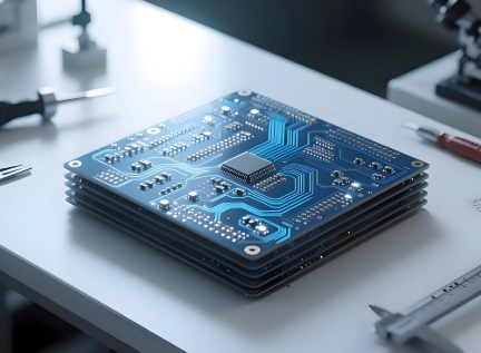
This step-by-step guide explains the complete PCB assembly process for engineers, procurement teams, and industrial buyers. Learn every stage from stencil creation to functional testing, with professional details to ensure high-quality, reliable electronic assemblies for prototypes and mass production.
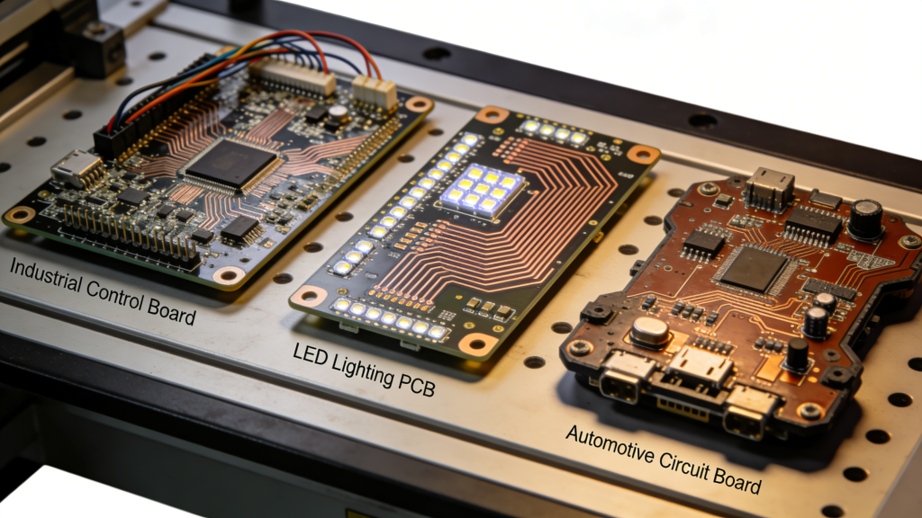
What transforms a bare printed circuit board into a fully functional electronic module for industrial, automotive, medical, or consumer devices? That is the role of the professional PCB assembly process, also known as PCBA.
This guide breaks down all 10 critical stages of PCB assembly with technical precision. Whether you are an R&D engineer validating a new prototype, a purchasing manager sourcing high-volume production, or a business owner seeking a reliable manufacturing partner, understanding these steps helps you avoid costly errors and ensure consistent quality.
For engineers: Focus on Steps 1–5 (stencil, paste, placement, reflow, AOI) and Step 7 (X-ray for BGAs).
For procurement & management: Prioritize Steps 8–10 (selective soldering, final inspection, packaging) for quality control and on-time delivery.
We use fully automated SMT production lines, in‑house AOI/SPI inspection, and lead‑free reflow soldering to deliver precision at every stage. By the end of this guide, you will understand how professional PCB assembly turns your design into a ready‑to‑use product.
Get a Quick PCB Assembly Quote
SMT Stencil Creation
Before solder paste is applied, a precision laser‑cut stainless steel stencil is manufactured to match your PCB pad layout. The stencil’s apertures align exactly with the board’s pads to control solder paste deposit position and volume.
This step directly determines solder joint quality. Misaligned, oversized, or undersized apertures cause weak joints, bridging, or missing solder — leading to failures later in PCB assembly.
We use laser‑cut stencils with ±0.01mm accuracy to support fine‑pitch components including 0.4mm QFPs and BGAs.
Solder Paste Printing & 3D SPI Inspection
The stencil is fixed onto the PCB, and an automated printer deposits lead‑free solder paste (typically SAC305) onto the pads. A squeegee ensures uniform paste transfer through the stencil apertures.
Immediately after printing, a 3D Solder Paste Inspection (SPI) system verifies paste volume, alignment, and height consistency. This prevents defects before components are placed.
SPI is a critical control point in PCB assembly — too little paste causes open joints; too much causes short circuits.
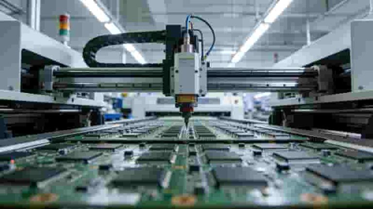
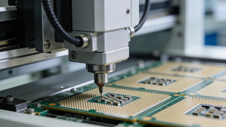
Automated Component Placement
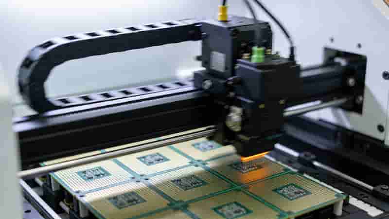
Populated PCBs move to high‑speed pick‑and‑place machines. Vacuum nozzles pick components from feeders and place them with ±0.05mm accuracy (±0.025mm for fine‑pitch parts).
Placement uses Gerber or centroid data with optical alignment to fiducial markers. High‑volume lines place up to 30,000 components per hour.
Precise placement avoids tombstoning, misalignment, and poor solder contact during reflow — key to reliable PCB assembly.
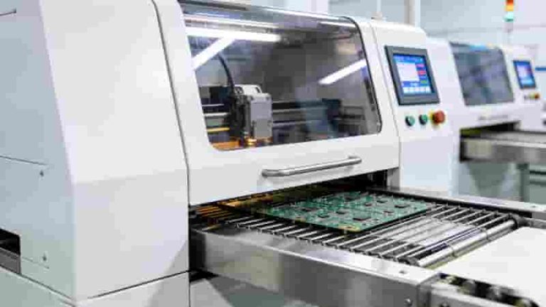
Reflow Soldering
Boards enter a multi‑zone reflow oven with controlled thermal profiling. Lead‑free solder paste melts and forms permanent, strong electrical and mechanical joints.
| Zone | Temperature | Purpose |
|---|---|---|
| Preheat | 150–180°C | Activate flux, remove solvents |
| Soak | 180–200°C | Thermal equilibrium across board |
| Reflow Peak | 235–245°C | Melt solder alloy, form joints |
| Cooling | Ramp to < 220°C | Solidify joints, avoid thermal shock |
Each new PCB uses a KIC thermal profiler to validate the reflow profile before mass production — a standard for professional PCB assembly.
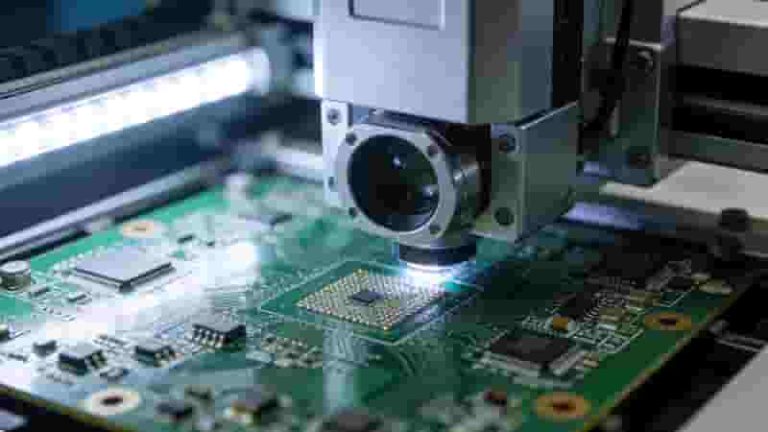
Automated Optical Inspection (AOI)
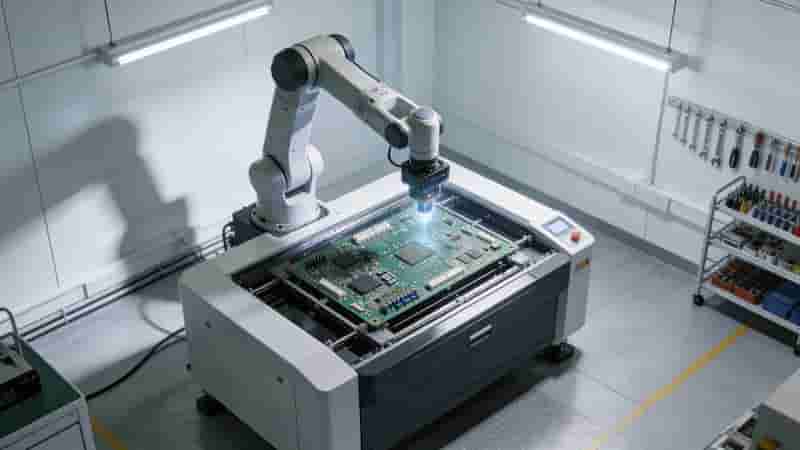
After reflow, 3D AOI systems scan the board to detect defects including missing components, wrong parts, polarity errors, bridging, insufficient solder, and tombstoning.
AOI inspects more than 95% of visible solder joints and is a primary quality gate in PCB assembly. Defects are flagged early to reduce rework and scrap.
Statistical Process Control (SPC)
SPC is a data‑driven system that monitors SPI, pick‑and‑place, reflow, and AOI in real time. It tracks CPK, drift, and repeatable errors to prevent defects before they occur.
Data is logged against IPC‑A‑610 standards for full traceability. SPC improves first‑pass yield, lowers costs, and ensures consistency from prototypes to mass production.
This level of control separates professional PCB assembly services from standard manufacturers.
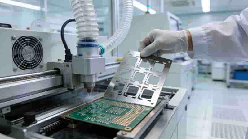
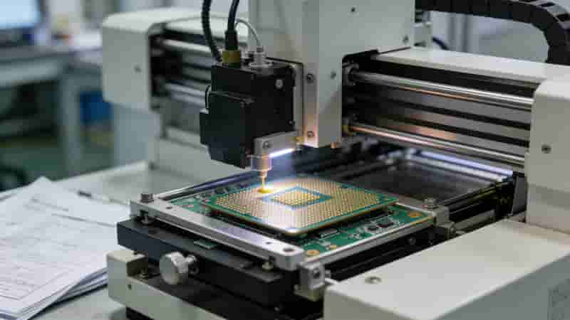
X-Ray Inspection (AXI)
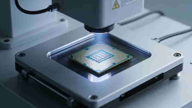
X-ray inspection reveals hidden joints under BGAs, QFNs, LGAs, and shielded components. It detects voids, bridging, missing solder balls, and head‑in‑pillow defects invisible to AOI.
For high‑reliability industries (automotive, medical, aerospace), X-ray is mandatory. We provide void‑percentage reports and 3D CT scanning for critical PCB assembly projects.
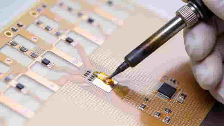
Selective Soldering for THT Components
Through‑hole components (connectors, transformers, capacitors) require selective soldering. A programmable mini‑solder wave targets only THT leads without damaging SMT components.
The process uses nitrogen to prevent oxidation and produce clean, consistent joints. It is the standard for mixed‑technology (SMT + THT) PCB assembly.
| Item | Manual Soldering | Selective Soldering |
|---|---|---|
| Consistency | Operator‑dependent | Programmed & repeatable |
| Quality | Risk of cold joints | Stable, IPC‑compliant |
| Speed | Slow | High throughput |
Cleaning, Final Inspection & Packaging
Boards are cleaned with deionized water to remove flux residues. Final visual inspection (FVI) verifies compliance with IPC‑A‑610.
Boards are packaged in ESD‑safe, moisture‑barrier bags with desiccant and anti‑static foam to ensure safe global shipping.
Proper packaging protects PCB assembly quality during long‑distance transport for export orders.
Functional Testing & Continuous Improvement
Functional testing validates complete electrical performance. Options include flying probe test, ICT, JTAG boundary scan, and custom functional testing.
Defects are repaired per IPC‑7711/7721. Test data and feedback drive DFM improvements to optimize future PCB assembly runs.
This closed‑loop system ensures long‑term reliability and cost efficiency.
Summary
The 10‑step PCB assembly process transforms bare PCBs into reliable, production‑ready electronic assemblies. Professional quality relies on precision equipment, real‑time inspection, SPC, IPC standards, and closed‑loop improvement.
From quick‑turn prototypes to high‑volume mass production, a controlled, transparent process ensures consistent quality, on‑time delivery, and cost efficiency for global industrial buyers.
Start Your PCB Assembly Project
Request a free quote, DFM review, or custom solution for your PCB assembly needs. We support prototypes, medium volumes, and mass production for global export.
Email for Quote
Upload Gerber & BOM
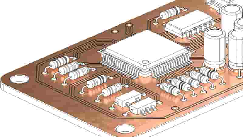
Surface Mount Technology (SMT): Advantages, Limitations & Applications
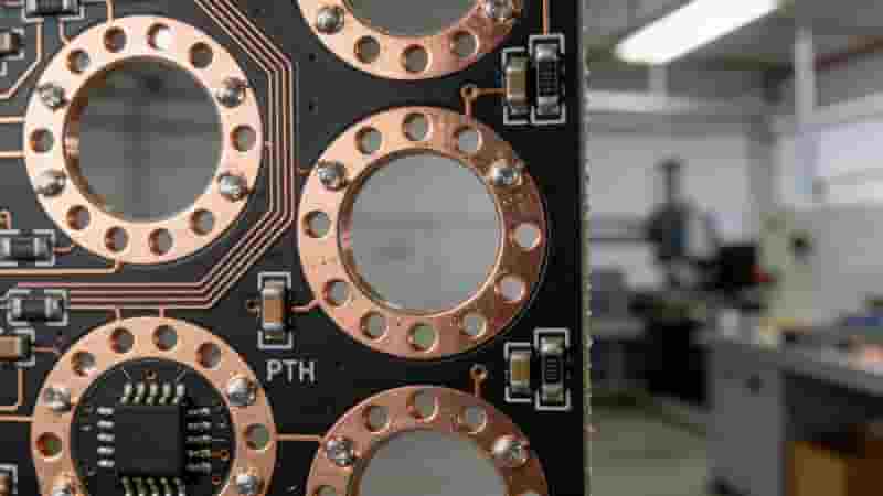
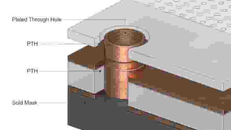
Understanding Plated Through Holes (PTH) for Printed Circuit Boards
Single-layer PCB vs. Double-sided PCB: How to Choose?
HASL: Hot Air Solder Leveling for PCB Surface Finish
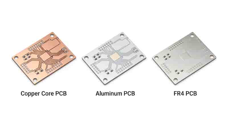
Why Choose FR-4 as Your PCB Material in 2025? The Definitive Engineer’s Guide