Flexible PCB coverlay is a protective polyimide film that protects FPC copper circuits while keeping full flexibility. Learn materials, thickness, comparison with solder mask, manufacturing, and selection for industrial and medical applications.
What Is Flexible PCB Coverlay?
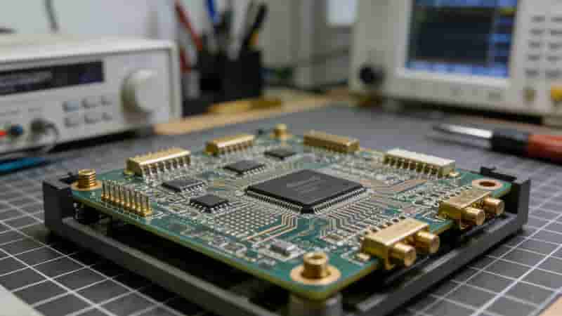
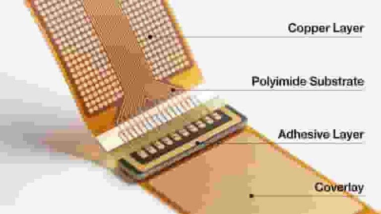
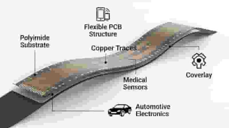
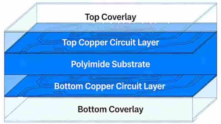
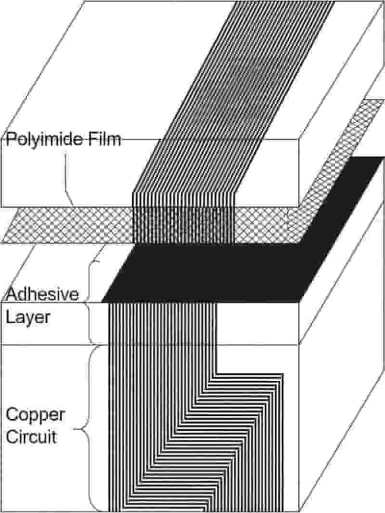
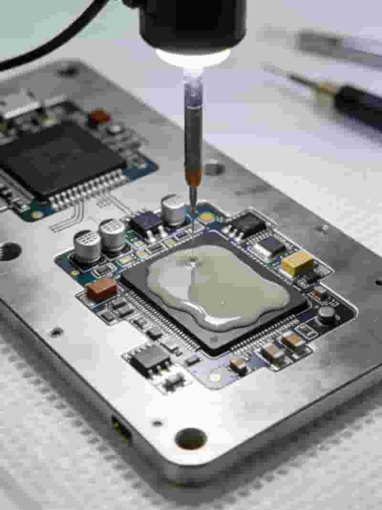
A flexible PCB coverlay, also known as FPC cover layer, is a key protective part for flexible printed circuits. It is made of polyimide film and flexible adhesive, which insulates and protects copper traces from moisture, dust, chemicals and mechanical stress while keeping the FPC bendable and foldable.
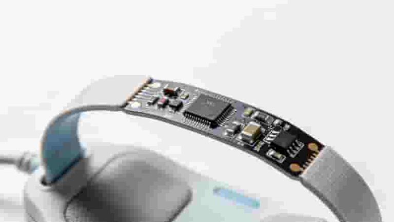
Different from rigid PCB solder masks, flexible PCB coverlay is designed for dynamic bending use, making it necessary for wearables, automotive electronics, medical devices and consumer electronics.
Key Functions of Flexible PCB Coverlay
- Protects copper circuits from corrosion, abrasion and environmental damage
- Provides high dielectric strength at about 3kV per mil thickness
- Keeps full flexibility for repeated bending and folding
- Improves FPC reliability and service life in harsh environments
- Meets industrial standards for medical, automotive and aerospace use
Flexible PCB Coverlay Thickness Options
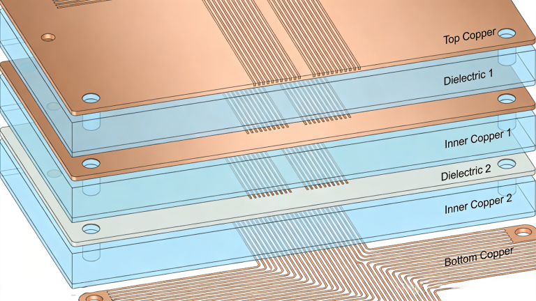
Flexible PCB coverlay thickness directly affects flexibility, durability and performance. Standard combinations include polyimide film and adhesive layers:
| Polyimide Thickness | Adhesive Thickness | Total Thickness | Best Application |
|---|---|---|---|
| 0.5 mil | 0.5 mil | 1.0 mil | Ultra-flexible wearables |
| 1.0 mil | 1.0 mil | 2.0 mil | Standard consumer electronics |
| 2.0 mil | 1.0 mil | 3.0 mil | Rugged automotive & industrial |
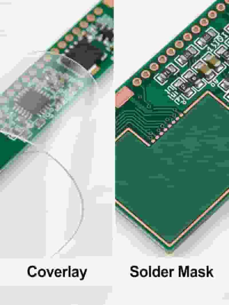
Coverlay vs Solder Mask: Key Differences
Both protect circuits, but flexible PCB coverlay and solder mask serve different design goals:
| Feature | Flexible PCB Coverlay | Solder Mask |
|---|---|---|
| Material | Polyimide + adhesive | Liquid epoxy polymer |
| Flexibility | High supports dynamic bending | Limited for rigid PCBs |
| Minimum Dam Size | 10 mils | 4 mils |
| Best For | FPC & rigid-flex boards | Rigid PCBs & fine-pitch parts |
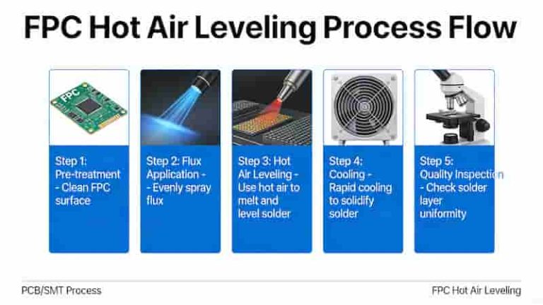
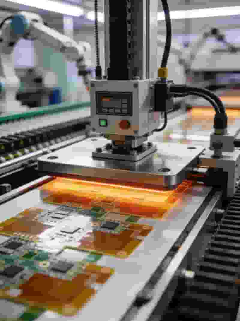
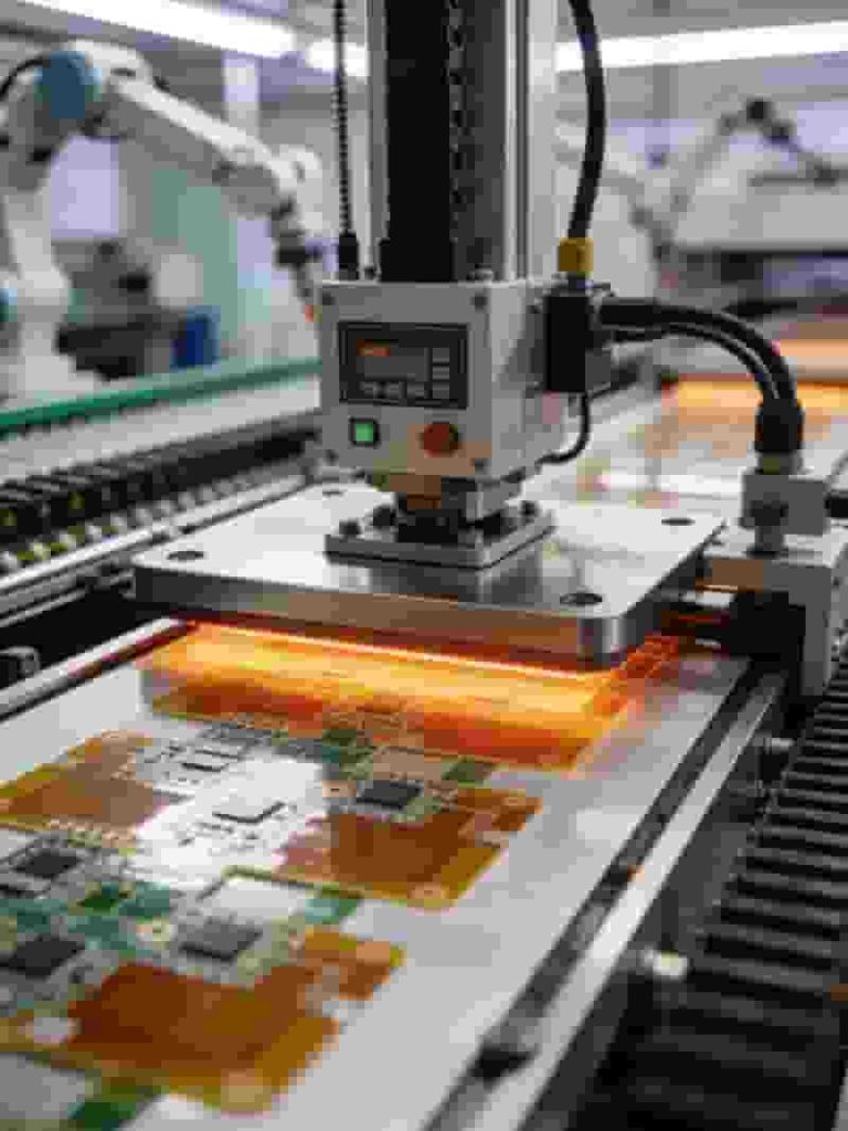
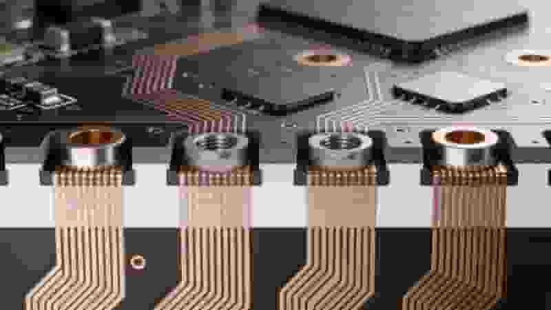
Flexible PCB Coverlay Manufacturing Process
- Material Selection: High-temperature polyimide film and acrylic or epoxy adhesive
- Precision Cutting: Laser or die-cut openings for pads, vias and components
- Alignment: Accurate placement on FPC with fiducial markers
- Lamination: Heat and pressure bonding for bubble-free adhesion
- Curing & Inspection: AOI check, flexibility test and dielectric validation
Industry Applications of Flexible PCB Coverlay
Flexible PCB coverlay supports reliable performance in high-demand industries:
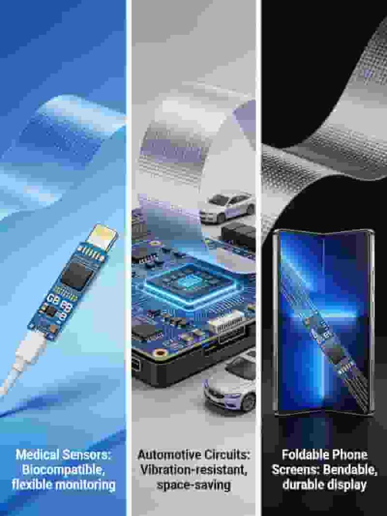
- Consumer Electronics: Foldable phones, wearables, wireless earbuds
- Medical Devices: Implantable sensors, wearable monitors, diagnostic tools
- Automotive: Sensors, lighting, dashboard circuits, infotainment systems
- Aerospace & Defense: Satellite circuits, avionics, drone controls
- Industrial & 5G: Robotics, high-speed antennas, flexible solar panels
How to Select the Right Flexible PCB Coverlay
Choose coverlay based on these important factors:
- Bending radius requirement: thinner film for tighter bending
- Environment exposure: thicker layers for harsh conditions
- Dielectric strength needs for high-voltage circuits
- Copper weight and circuit density
- Industry compliance for medical, automotive and aerospace
Conclusion
Flexible PCB coverlay is an essential component for reliable and long-lasting flexible circuits. It balances protection, insulation and flexibility to meet modern electronic needs. Choosing the right material and thickness ensures the best performance for your FPC design.
Need Professional Flexible PCB Support?
Get FPC design, material selection and manufacturing support for your global export projects.
Request Free Quote & DFM Check
Aluminum PCB Manufacturing & Assembly Services
PCB Vias: Complete Guide to Types, Design, Reliability & Applications

PCB Components Purchasing Services | Global Electronic Components SourcingPCB
The Essentials of Microvias – Enabling Miniaturization in PCBs
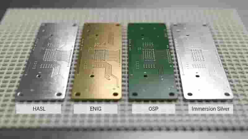
Choosing the Right PCB Surface Finish for Your Project in 2025