PCB vias are essential vertical interconnects that enable layer transitions in multilayer printed circuit boards. This professional guide covers via definitions, core types, manufacturing processes, reliability factors, advanced structures, and best practices for engineers and global buyers.
What Are PCB Vias
A PCB via is a plated vertical electrical connection that routes signals, power, and ground between different layers of a printed circuit board. PCB vias are foundational components for multilayer PCB design, enabling high-density routing and complex circuit functionality.
Without PCB vias, modern high-density interconnect (HDI) PCBs and advanced electronic devices would not be possible. They solve routing congestion, improve signal integrity, enhance thermal management, and support miniaturization trends in electronics.
Main Types of PCB Vias
There are three primary categories of PCB vias used in commercial and industrial PCB manufacturing:
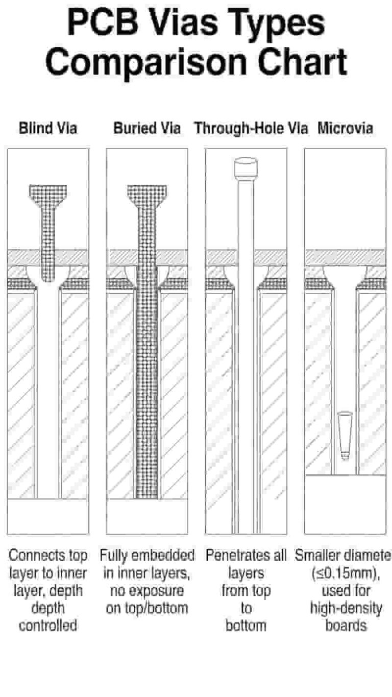
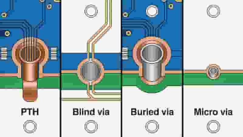
1. Plated Through-Hole Vias (PTH)
Plated Through-Hole Vias span the entire thickness of the PCB, connecting all layers from top to bottom. They are the most common and cost-effective via type for standard multilayer PCBs.
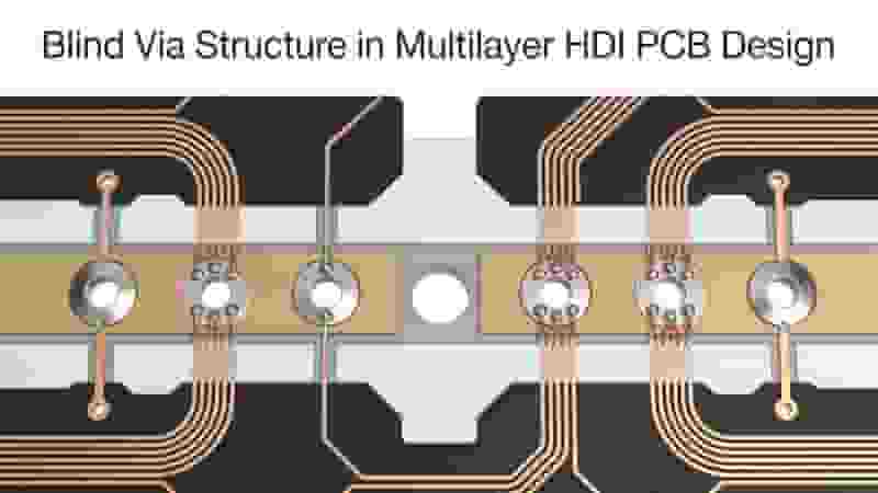
2. Blind & Buried Vias
Blind Vias connect an outer layer to one or more inner layers but do not penetrate the entire board. Buried Vias exist only between inner layers, with no exposure on outer surfaces. Both optimize routing density for HDI designs.
3. Micro Vias
Micro Vias are laser-drilled vias with diameters typically below 0.15mm. They are critical for high-frequency, high-density PCBs used in 5G, automotive, and consumer electronics.
| Via Type | Diameter | Best For | Cost |
|---|---|---|---|
| Plated Through-Hole | 0.2mm – 1.0mm | Standard multilayer PCBs | Low |
| Blind / Buried | 0.15mm – 0.3mm | HDI PCBs, medium density | Medium |
| Micro Via | ≤0.15mm | High-frequency, 5G, automotive | High |
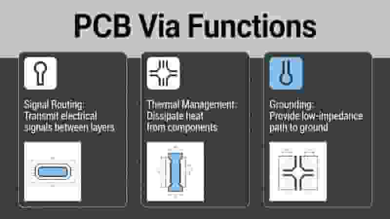
Key Functions of PCB Vias
PCB vias perform multiple critical roles in modern circuit board design:
- Interlayer Signal Routing: Connect traces between different PCB layers to resolve routing conflicts.
- Power & Ground Delivery: Provide stable electrical paths for power distribution and grounding.
- Thermal Management: Transfer heat from components to inner or outer copper planes for cooling.
- Signal Integrity: Support high-speed transmission with controlled impedance and minimal stubs.
- Component Mounting: Serve as connection points for through-hole component leads.
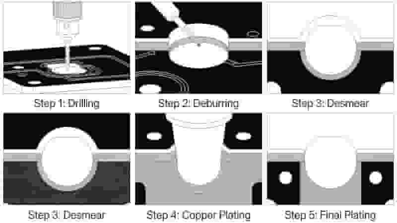
PCB Via Construction & Materials
High-quality PCB vias require precise manufacturing processes to ensure reliability and performance:
- Drilling: Mechanical drilling for standard vias; laser drilling for microvias and HDI designs.
- Desmear & Activation: Clean and prepare hole walls for reliable copper adhesion.
- Electroless Copper Plating: Deposit thin conductive copper layer on via walls.
- Electroplating: Build up copper thickness to meet conductivity requirements.
- Filling & Capping: Optional epoxy filling for improved thermal performance and reliability.
PCB Via Reliability & Failure Modes
PCB via reliability directly impacts the lifespan and performance of electronic products. Common failure modes include:
- Copper barrel cracking due to thermal expansion mismatch
- Incomplete plating leading to open circuits
- Pad lifting or delamination from mechanical stress
- Via voids caused by improper filling or plating
We use strict quality control and reliability testing (thermal cycling, vibration, and electrical testing) to ensure all PCB vias meet international industrial standards.
Advanced PCB Via Technologies
Advanced via technologies push the limits of PCB performance for demanding applications:
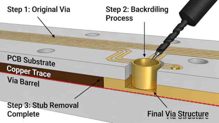
Backdrilled Vias
Remove unused via stubs to minimize signal reflection and improve high-speed signal integrity.
Filled & Capped Vias
Enhance thermal conductivity, prevent solder wicking, and improve structural stability.
Via-in-Pad (VIP)
Maximize routing space by placing vias directly under component pads, ideal for BGA and fine-pitch devices.
Conclusion
PCB vias are indispensable components in modern multilayer PCB design. From basic PTH vias to advanced microvias and via-in-pad structures, they enable the miniaturization, high performance, and reliability required by today’s electronics industry.
Understanding PCB via types, functions, and reliability factors helps engineers and buyers make informed decisions to optimize PCB performance, cost, and manufacturability.
Get Professional PCB Via Design & Manufacturing Support
We provide high-quality multilayer PCB manufacturing with reliable PCB vias for global industrial clients. Contact us for custom PCB solutions, quotes, or technical support.
Inquire Now | Get Free Quote
Blind Vias & Buried Vias in PCBs – The Complete Engineering Guide
PCB Materials Classification & Substrate Selection Guide
What Are PCB Boards Made Of? Complete Materials Guide for Engineers & Buyers
Single-Sided Flexible PCB Fabrication & Assembly Services
Flexible PCB Stiffeners: Materials, Benefits & Industrial Uses