Advanced controlled impedance PCB manufacturing for high-speed, RF and telecom designs, delivering precise 50 Ω / 90-100 Ω impedance, tight tolerances and fast global turnaround.
Tight-tolerance controlled impedance: 50 Ω single-ended and 90/100 Ω differential traces engineered for consistent signal integrity.
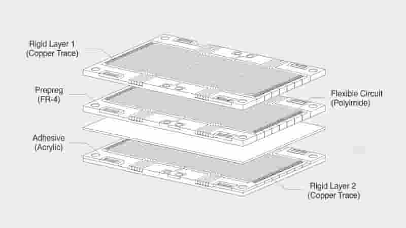
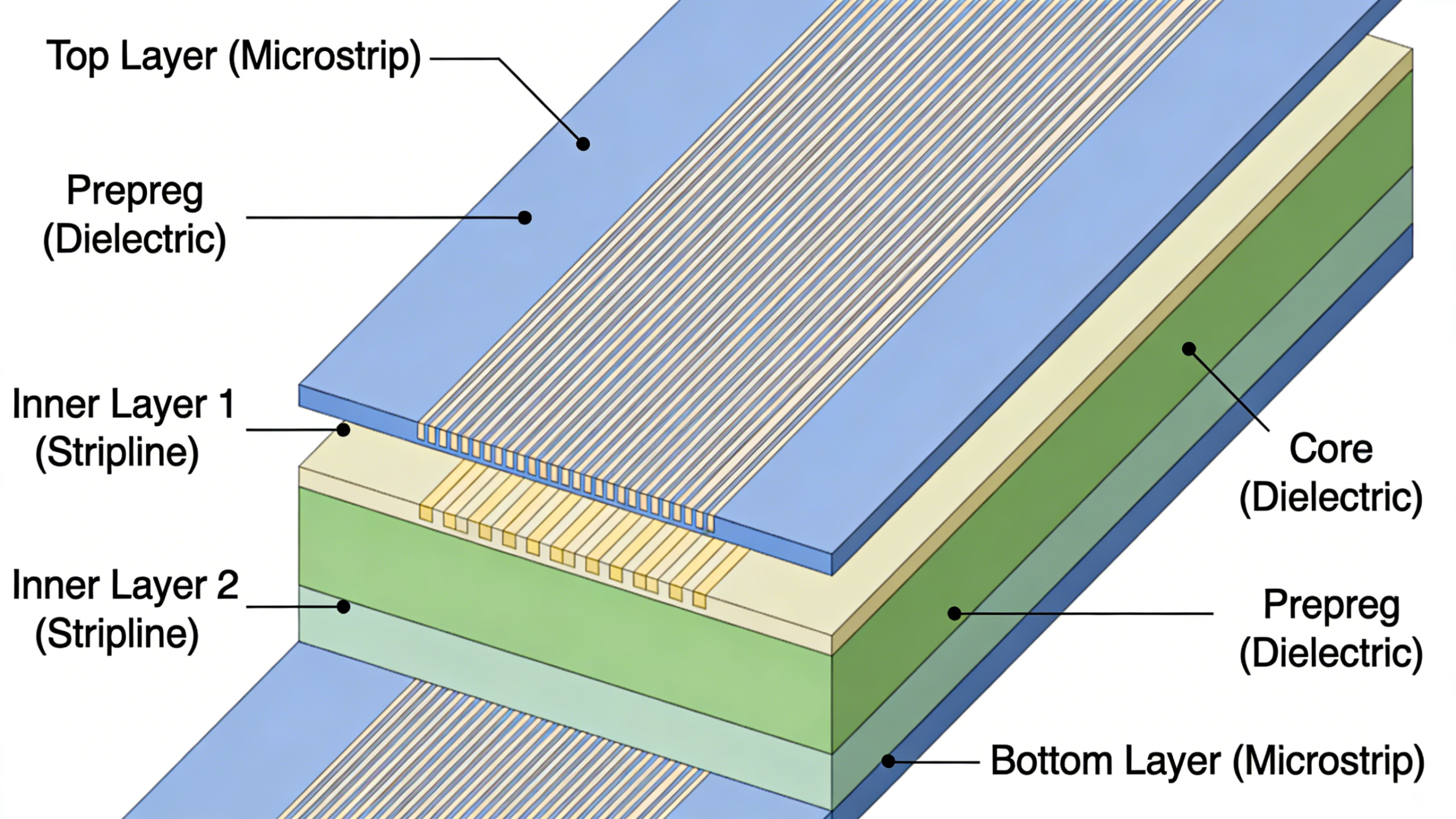
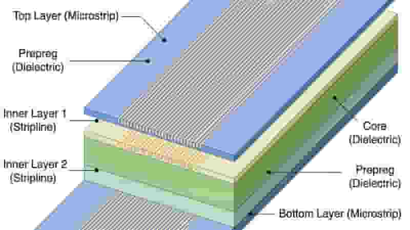
Multilayer stackups with FR-4 and high-frequency materials (Rogers, hybrid) for complex high-speed designs.
Full engineering support for stackup, routing and DFM review before production.
Impedance coupons, TDR testing and detailed measurement reports provided for validation.
Get Impedance Control PCB Quote
Send Your Gerber Files
ISO, UL and RoHS certified PCB manufacturer, supporting prototypes, small runs and volume production with reliable impedance control.
Impedance Control PCB Capabilities
Our impedance control PCB fabrication service supports a wide range of high-speed and RF designs, from prototypes to volume production, with stable, repeatable impedance performance across multilayer stackups.
| Capability | Typical Specification |
|---|---|
| Impedance types | 50 Ω single-ended, 75 Ω video, 90 Ω and 100 Ω differential pairs, coplanar waveguides |
| Target tolerance | ±10% standard, tighter available for critical high-speed channels |
| Layer count | 4-layer to complex high-density multilayer designs |
| Materials | FR-4, Rogers, hybrid high-frequency laminates |
| Stackup & geometry | Microstrip, stripline, dual-stripline optimized for impedance control |
| Testing & reporting | Impedance coupons, TDR measurement, full test reports |
Impedance Control PCB Specification Overview
When Do You Need Controlled Impedance PCBs?
Controlled impedance becomes critical whenever high-speed or high-frequency signals travel across the PCB without distortion, reflections or timing errors.
If your design operates at hundreds of megahertz or uses fast edge-rate digital interfaces, you need impedance control to maintain signal integrity and reliable system performance.
Typical Applications
- Telecom and networking equipment (switches, routers, base stations)
- High-speed computing systems (100 MHz and above)
- RF and microwave communication modules
- High-resolution imaging and analog video systems
- Data acquisition and test & measurement instruments
Typical Signal Types
- High-speed differential pairs (LVDS, USB, PCIe, Ethernet)
- High-speed clocks and critical timing signals
- RF transmission lines requiring matched impedance control
- Long-distance signal traces matching cable/connector impedance
Impedance Control PCB Industry Applications
How to Specify Impedance Control for Your PCB Order
To achieve target impedance, our engineering team needs clear design, material and performance requirements. Providing these details avoids delays and optimizes stackup and geometry.
Key Electrical Requirements
- Target impedance values (50 Ω single-ended, 90/100 Ω differential)
- Transmission line type (single-ended, differential, microstrip, stripline)
- Impedance tolerance (standard ±10% or tighter for critical nets)
Stackup & Material Information
- Proposed layer stackup, copper weights and dielectric thickness
- Base material (FR-4, Rogers or hybrid high-frequency laminates)
- Overall board thickness and mechanical constraints
Design Files & Documentation
- Complete Gerber / ODB++ files with impedance notes
- Stackup drawing, schematics and simulation data (if available)
- Test and reporting requirements (coupons, TDR, reports)
How We Fabricate Impedance Control PCBs
Our process tightly controls trace geometry, dielectric thickness and material properties to ensure finished boards match your target impedance control requirements.
1. Engineering Review & Stackup Optimization
CAM and SI engineers review Gerber files, impedance tables and stackups to confirm manufacturability.
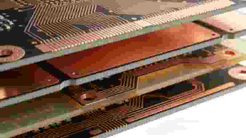
2. Precision Lamination & Layer Buildup
Controlled copper and dielectric thickness to match impedance models.
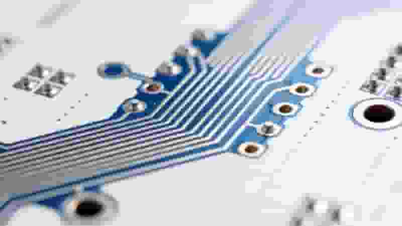
3. Controlled Imaging & Etching
High-resolution processes maintain trace width/spacing for impedance-critical lines.
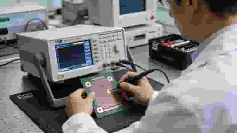
4. Impedance Coupons & TDR Measurement
Coupons tested via TDR to validate impedance control within tolerance.
5. Final Inspection & Documentation
Electrical test, visual inspection and full quality reports provided.
Impedance Control PCB Fabrication Flow
Why Choose Us for Impedance Control PCBs
- Proven high-speed/RF expertise in telecom, networking and RF applications requiring impedance control
- Dedicated engineering support for stackup, impedance and DFM before production
- Controlled processes + TDR validation for consistent, repeatable results
- Flexible quantities from prototypes to mass production
- Certified quality (ISO, UL, RoHS) with global delivery
- Transparent technical communication to keep projects on track
Impedance Control PCB Engineering Support
Ready to Build Your Impedance Control PCB?
Our team supports stable, repeatable impedance control from prototype to volume production.
Get Impedance Control PCB Quote
Email Your Gerber Files
Recommended PCB Services
Double-Sided PCB Manufacturing
High Tg PCB Manufacturing
Quick Turn PCB Fabrication
Metal Core PCB Manufacturing
BGA PCB Manufacturing
SMT PCB Assembly Service
Get DFM-optimized impedance control PCB in as fast as 24 hours. 100% quality guaranteed.
Ultimate Guide to Multilayer PCB Layer Stackup & Thickness | Standard 4–14 Layer Configurations
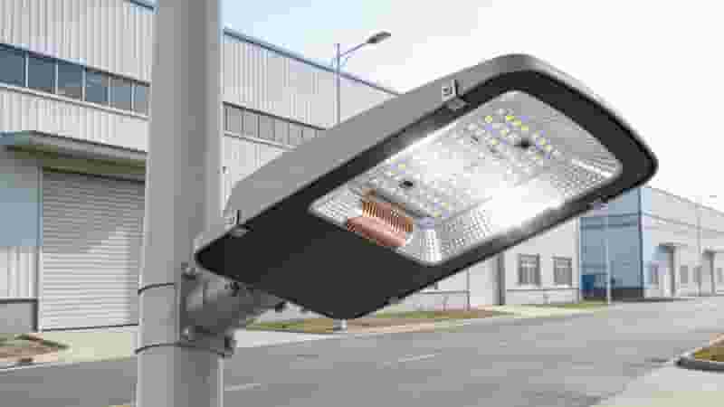
High-Performance Copper Core PCBs for LED and Power Applications
PCB Design Guidelines for Manufacturing & IPC Compliance
What Is Prototype PCB Assembly
PCB Manufacturing Process Part 1: MI, Cutting & Drilling – Complete Industrial Guide