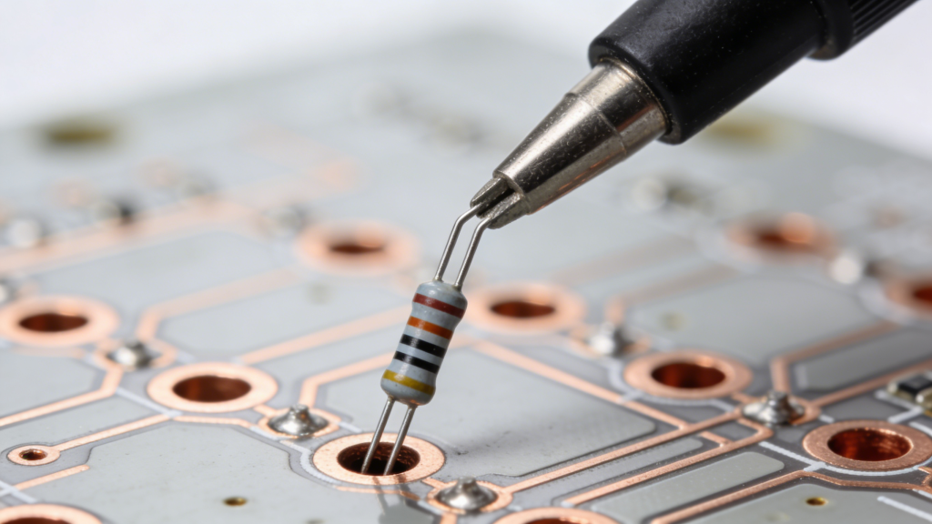
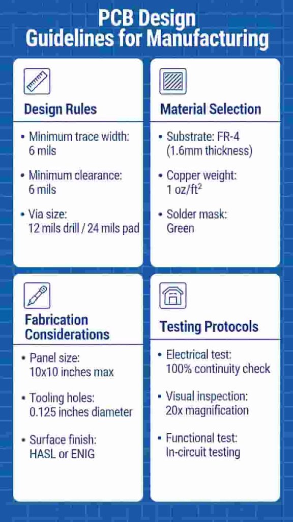
Printed circuit boards are a foundational component of modern electronics. Following professional PCB design guidelines ensures reliability, manufacturability, cost efficiency, and compliance with global production standards.
Board Size & Thickness Specifications
PCB manufacturers follow maximum panel size limits, which directly impact mass production efficiency and cost. Proper panelization maximizes board count and minimizes waste.
- Standard routing spacing between boards: 0.3″
- Processing border: 1.0″ to 2.0″ around the panel
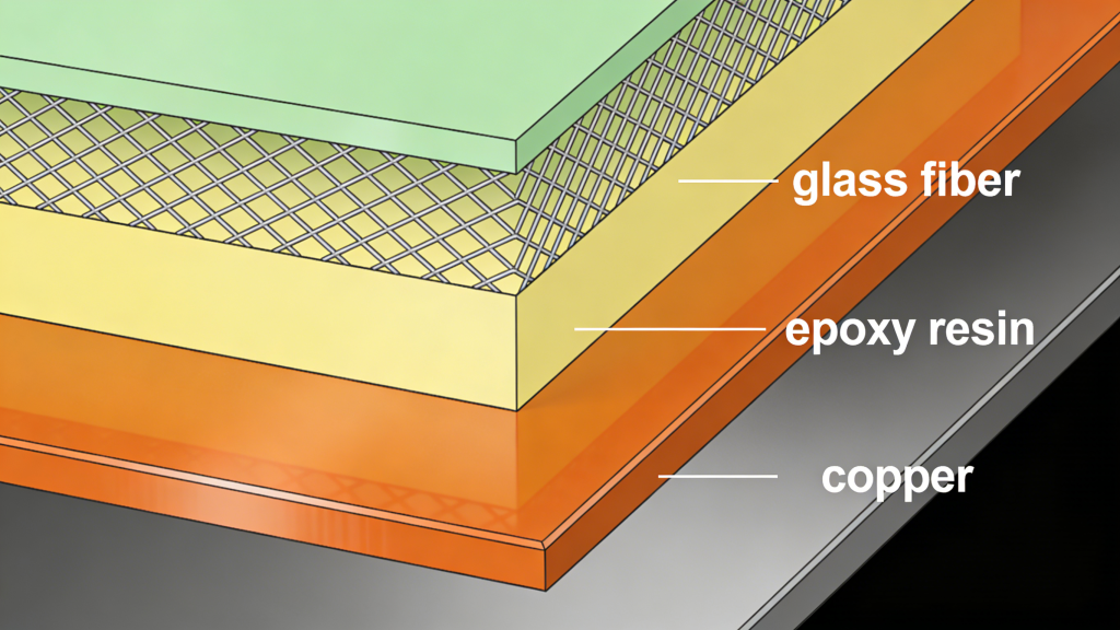
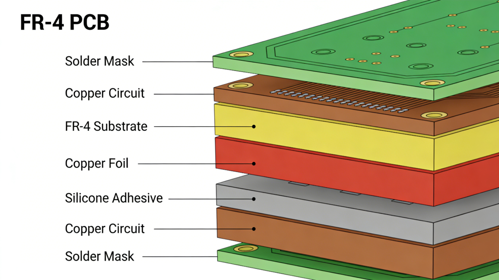
- Standard thickness: 0.062″ FR‑4
- Common thickness options: 0.010″, 0.020″, 0.031″, 0.092″
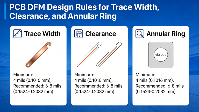
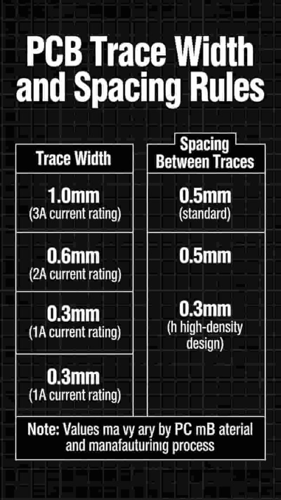
Trace Width & Spacing Rules
Trace width and spacing are critical to avoid open circuits, shorts, and assembly failures. These follow standard “x/y rules” where x = minimum trace width, y = minimum spacing.
- Standard industry rule: 8/8 mil
- High-density advanced capability: down to 2/2 mil
- Hand soldering recommendation: 10/10 mil
- Press‑n‑Peel: 12/12 mil works reliably
- Avoid 90° angles; use 45° or curved paths to reduce signal reflection
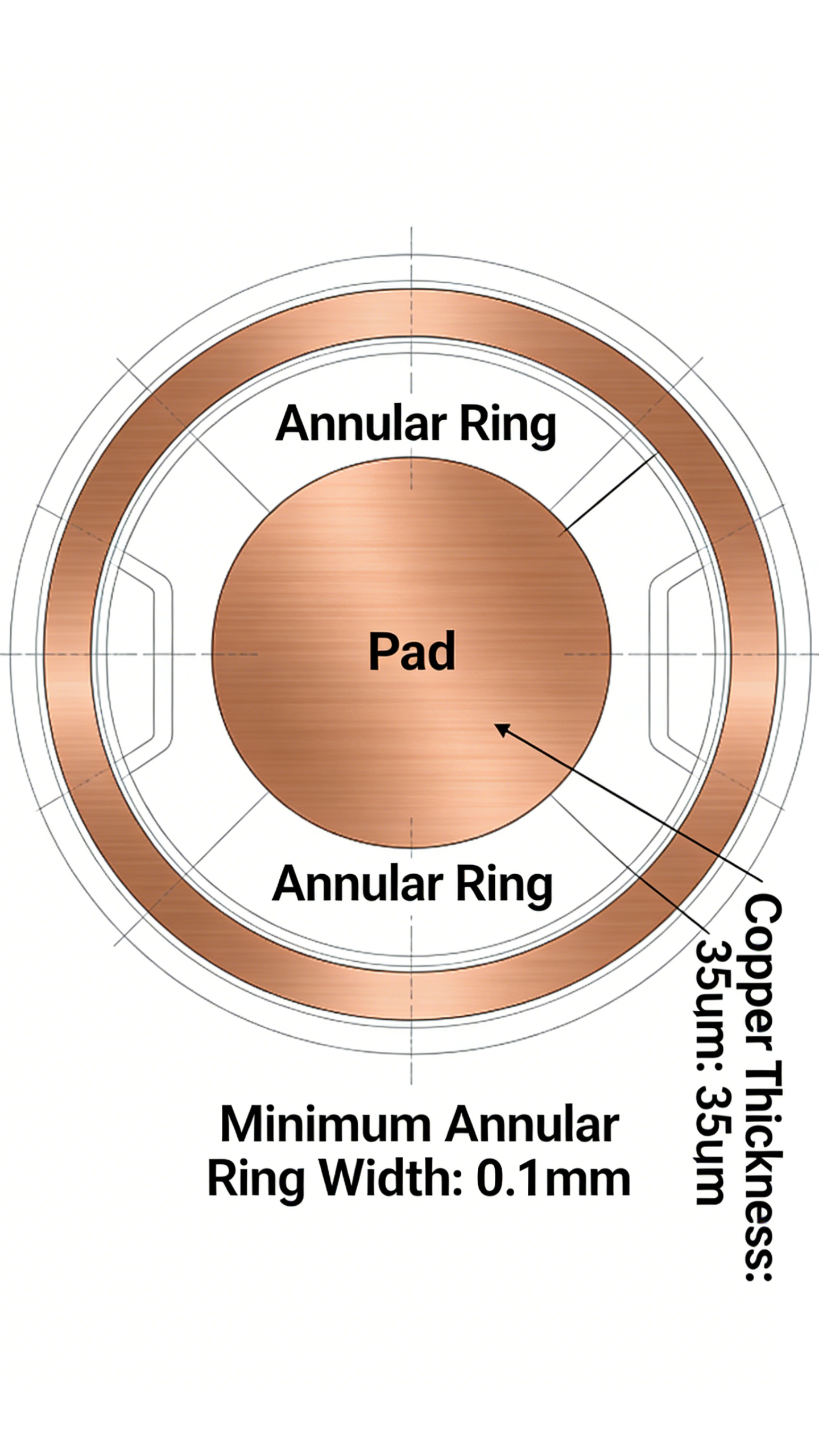
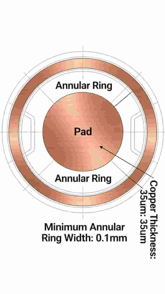
Pad Sizes & Hole Size Standards
Pad design affects solderability and manufacturing reliability. The annular ring prevents broken pads caused by drill deviation.
- Standard annular ring: 5 mil (0.005″)
- Example: 28 mil hole requires 38 mil pad
- Plated through‑hole reduces finished size by ~0.003″
- 2.5 mil annular ring is possible but not recommended for high reliability
Standard Drill Sizes & Finished Holes
| Drill Number | Hole Size (inch) | Finished Hole Size |
|---|---|---|
| 70 | 0.028″ | 0.025″ |
| 65 | 0.035″ | 0.032″ |
| 58 | 0.042″ | 0.039″ |
| 55 | 0.052″ | 0.049″ |
| 53 | 0.0595″ | 0.056″ |
| 44 | 0.086″ | 0.083″ |
| 1/8″ | 0.125″ | 0.122″ |
| 24 | 0.152″ | 0.149″ |
Hole Density & Full Drill Chart
Hole density affects cost and tool wear. Most factories charge extra for densities above 24 holes per square inch.
Full drill chart below is for engineering reference and global factory compatibility.
| Drill No. | Inches | Drill No. | Inches | Drill No. | Inches |
|---|---|---|---|---|---|
| 80 | .0135 | 53 | .0595 | 27 | .1440 |
| 79 | .0145 | 52 | .0635 | 26 | .1470 |
| 78 | .0160 | 51 | .0670 | 25 | .1495 |
| 77 | .0180 | 50 | .0700 | 24 | .1520 |
| 76 | .0200 | 49 | .0730 | 23 | .1540 |
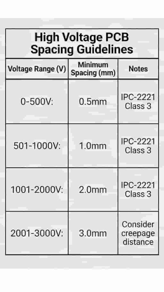
High-Voltage Trace Spacing Guidelines
High‑voltage PCB design requires strict spacing to avoid arcing and insulation failure. Values apply to internal/external conductors, solder mask, and conformal coating.
| Voltage Range | Internal (A1) | External Uncoated (A2) | Solder Mask (A4) |
|---|---|---|---|
| 0–15V | 0.004″ | 0.025″ | 0.005″ |
| 16–30V | 0.004″ | 0.025″ | 0.005″ |
| 51–100V | 0.004″ | 0.060″ | 0.005″ |
| 301–500V | 0.010″ | 0.100″ | 0.030″ |
| Over 500V | 0.0001″/V | 0.0002″/V | 0.00012″/V |
Electrical Design Parameters & Formulas
Professional PCB design guidelines include core electrical formulas for impedance, capacitance, and resistance used by industrial engineers worldwide.
- Conductor Capacitance: depends on dielectric constant, geometry, and spacing
- Conductor Resistance: based on trace width and copper properties
- Characteristic Impedance (Zo): critical for high‑speed signal integrity
- Microstrip Impedance: controlled for RF and high‑speed designs
Summary & DFM Quick Checklist
Following these complete PCB design guidelines ensures your boards are manufacturable, reliable, and cost‑effective for global export and mass production.
- Match board size to factory panel limits for best cost
- Use 8/8 mil or 10/10 mil trace rules for consistent production
- Maintain 5 mil annular ring for reliable pads
- Follow high‑voltage spacing rules for safety
- Control hole density to avoid extra charges
- Validate drill sizes, finished holes, and plating thickness
Get Expert PCB Support & Quote
Send your Gerber files for full DFM analysis, fast lead times, and competitive pricing for international orders.