This expert guide delivers 10 actionable PCB design for manufacturing best practices to lower production cost, improve yield, speed up assembly, and ensure high‑reliability PCBs for industrial, automotive, and high‑tech applications.
Introduction to PCB Design for Manufacturing
PCB design for manufacturing (DFM) is a core engineering methodology that aligns PCB layout with real‑world production capabilities. It reduces defects, cuts costs, shortens lead times, and improves reliability for mass production and prototyping alike.
Whether you are designing for consumer electronics, industrial controls, automotive, or medical devices, following DFM rules ensures your boards can be built efficiently by automated SMT and through‑hole assembly lines.
Why PCB DFM Is Critical
Weak DFM leads to assembly failures, high scrap rates, rework costs, and delayed launches. Common issues include tombstoning, misalignment, solder bridges, thermal failure, and depaneling damage.
By following industry standards including IPC‑A‑600, IPC‑2221, and IPC‑7351, you eliminate avoidable manufacturing risks and ensure consistent, high‑yield production.
10 Essential Tips for PCB Design for Manufacturing
1. Choose Available, Standard Components
Prioritize widely available, lead‑free, RoHS compliant components to avoid supply chain delays. Non‑standard parts increase cost and risk shortages. For high‑reliability projects, use components with clear MTBF data.
2. Standardize Component Values
Reuse identical resistors, capacitors, and connectors across designs. Standardization simplifies inventory, speeds programming for pick‑and‑place machines, and lowers overall PCB manufacturing cost.
3. Design for Automated SMT Assembly
Optimize for SMT and reflow soldering instead of manual assembly. Follow reflow profiles for SAC305 lead‑free solder to ensure strong, consistent joints.
4. Match Assembly to Production Volume
Use panelization for high volume and selective soldering for prototypes. Follow standard machine limits (330mm × 250mm for reflow) to avoid production jams and delays.
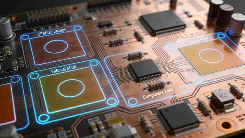
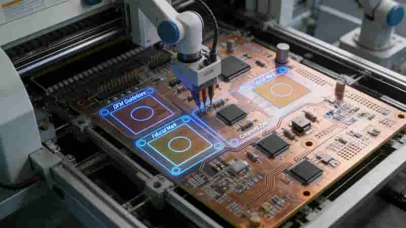
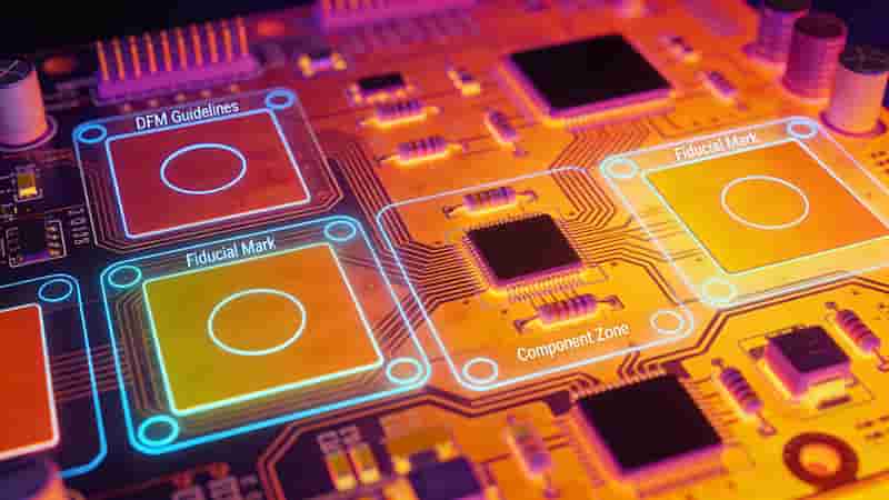
5. Use Clear Fiducials and Silkscreen
Place 1.0mm fiducials at board corners with 5mm edge clearance. Use legible silkscreen (minimum 0.8mm text) to help assembly and inspection systems work accurately.
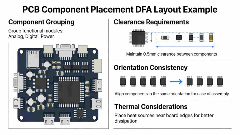
6. Optimize Component Placement
Keep 1–2mm clearance around BGAs and QFNs. Avoid heavy components near board edges to prevent mechanical stress and solder joint cracks.
7. Maintain Uniform Component Orientation
Align passives and ICs consistently to reduce tombstoning and placement errors. Pin 1 markings should follow assembly direction per IPC‑7351.
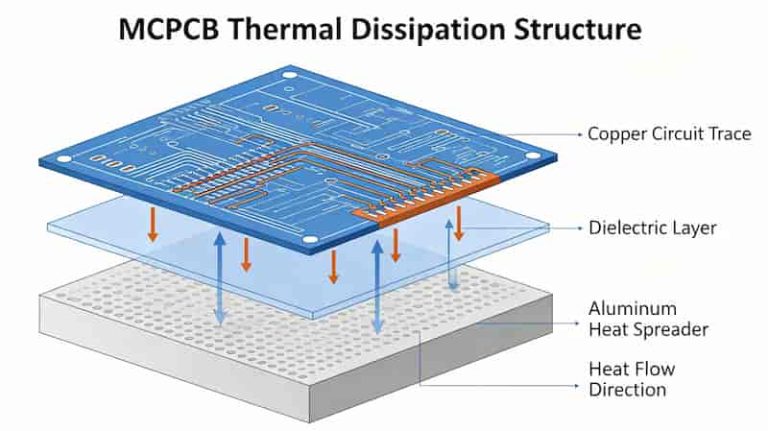
8. Prioritize Thermal Management
Place high‑power devices near edges or cooling zones. Use thermal vias (0.3mm) to ground planes for heat dissipation. Simulate thermal performance to avoid hotspots.
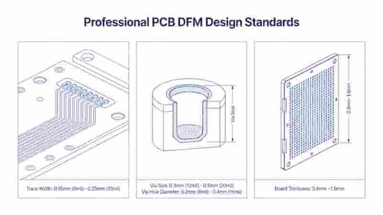
9. Define Robust Physical Specifications
Use standard thickness (1.6mm typical), limit warpage to 0.75%, and add 2–4 positioning holes. Stable physical design ensures compatibility with all PCB manufacturing equipment.
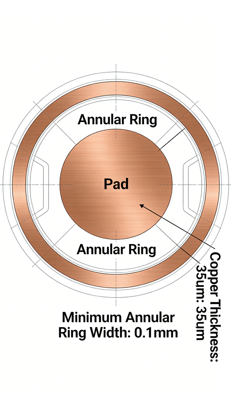
10. Optimize Panelization and Trace Routing
Use V‑groove or tab routing for safe depaneling. Maintain minimum trace width (0.15mm for 1oz copper) and keep traces 2mm from panel edges to prevent damage.
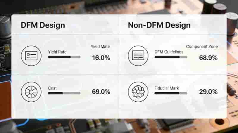
DFM vs Non‑DFM PCB Design Comparison
| Factor | Good DFM Design | Poor Non‑DFM Design |
|---|---|---|
| Production Yield | 98%+ | Below 85% |
| Assembly Cost | Standard & Low | High with Rework |
| Lead Time | Fast & On Schedule | Delayed |
| Reliability | High & Stable | Risk of Failure |
Advanced PCB Design for Manufacturing Tips
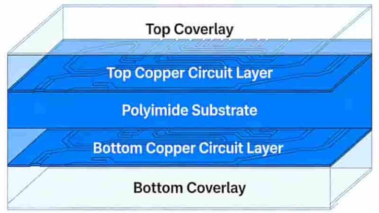
Include DFT test points for ICT inspection to speed up testing. Select high‑Tg FR‑4 or high‑frequency materials for demanding environments. For HDI PCBs, use microvias and stacked vias only if your manufacturing partner supports advanced capabilities.
Conclusion
Following these 10 tips transforms PCB design for manufacturing from an afterthought into a reliable, cost‑saving process. Better DFM means higher yield, lower cost, faster delivery, and more durable PCBs for global markets.
Get Expert PCB Manufacturing Support
We provide professional DFM review, PCB fabrication, and SMT assembly for global buyers. Send your Gerber files for a free quote and detailed design analysis.
Request Free DFM Check & Quote