PCB & PCBA Manufacturing Files: Complete Guide for Production & Quotation

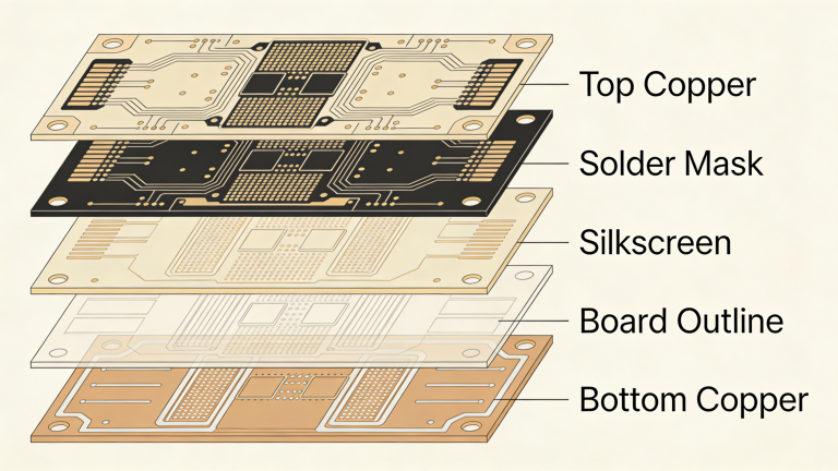
PCB Gerber File Structure and Layer Diagram

This guide details all essential PCB & PCBA manufacturing files, including Gerber files, BOM lists, NC Drill files, Centroid files, and other critical documents. It provides professional standards, format requirements, and technical parameters to ensure accurate quotes, error-free production, and reliable PCB assembly for global industrial buyers, engineers, and procurement teams.

Core Files for PCB Manufacturing

Professional PCB fabrication requires complete, standardized files to avoid production errors and ensure design consistency. The mandatory files include:

  • Gerber Files (RS-274X / Gerber X2) – Industry standard for layer imaging
  • NC Drill File (Excellon Format) – Defines hole positions and sizes
  • .BRD / .PCB / .PCBDOC Files – Native design source files
  • Stack-Up & Impedance Control Documents – For high-speed boards
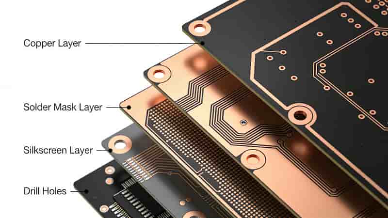
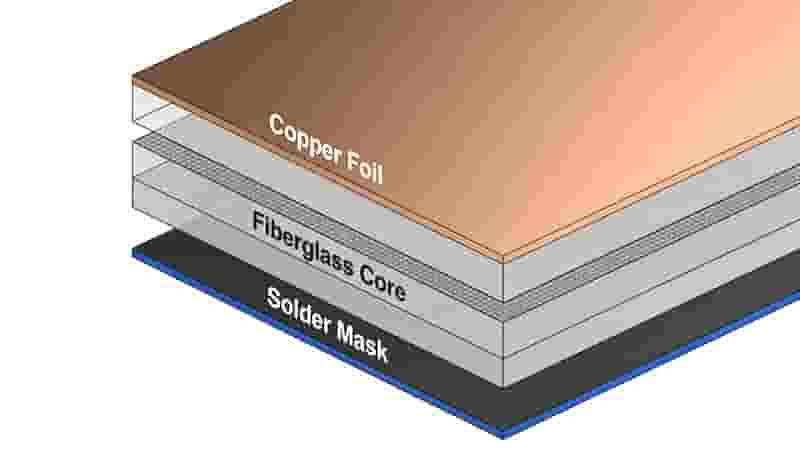
PCB Gerber File Structure and Layer Diagram

Gerber Files: Standards & Versions

Gerber is the global de facto standard for PCB image description. It defines copper layers, solder mask, silkscreen, and paste mask.

Gerber Format Versions

  • Gerber X2 – Latest version with integrated attribute data
  • RS-274X (Extended Gerber) – Most widely used industry format
  • RS-274D (Standard Gerber) – Obsolete, not recommended

Each layer requires one Gerber file. A typical 2-layer PCB needs 6 Gerber files: top/bottom copper, top/bottom solder mask, top/bottom silkscreen.
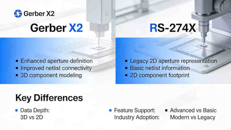
Gerber X2 vs RS-274X Comparison for PCB Manufacturing

NC Drill File (Excellon Format)

The NC Drill file provides precise drilling coordinates, hole sizes, and tool numbers. It must match Gerber layer data to avoid misalignment in PCB production.

Required Files for PCBA Assembly

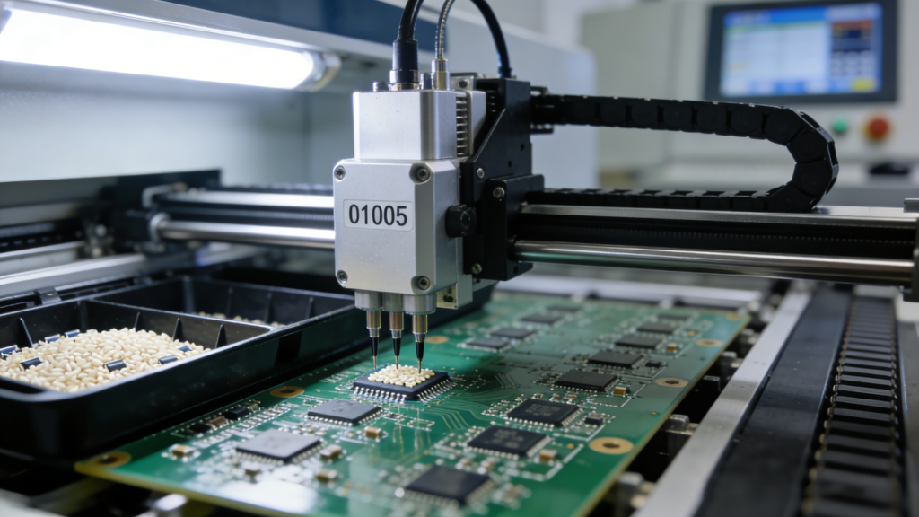
Reliable PCBA assembly depends on complete, accurate files for SMT placement, component sourcing, and quality control.

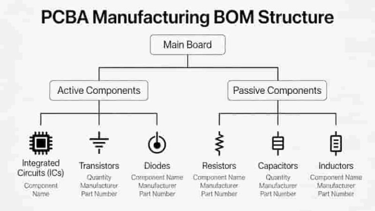
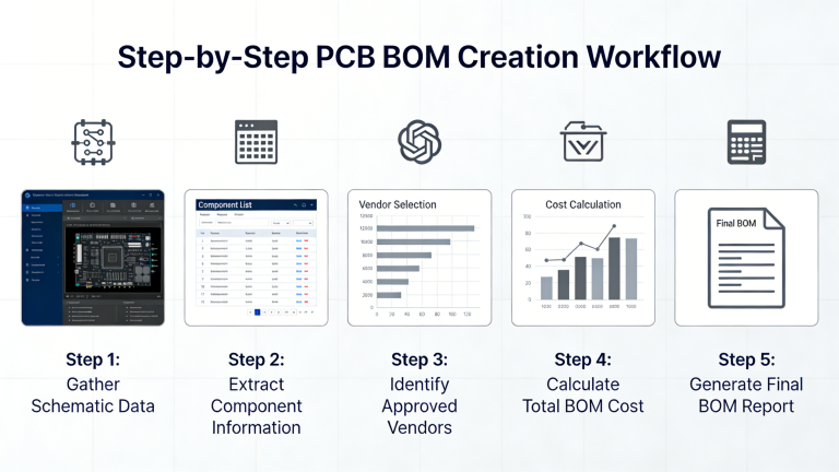
Bill of Materials (BOM)

A complete BOM includes: reference designators, quantity, description, manufacturer part number (MPN), package, and tolerance.

Centroid File (Pick & Place / XY Data)

This file defines X/Y coordinates, rotation, and layer (top/bottom) for each SMT component, enabling automated SMT assembly.
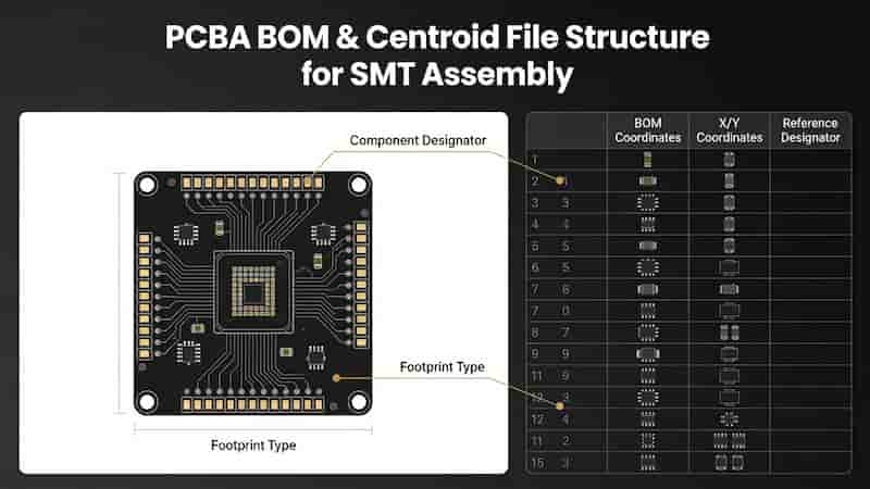
PCBA BOM and Centroid File Structure for SMT Assembly

Additional PCBA Documents

  • Assembly Drawing (component polarity & placement)
  • Test Guide & Fixture Information
  • IC Programming Files (if required)

Inspection & Test Documents

Quality assurance files ensure PCB and PCBA meet IPC standards and customer specifications.

  • KLARF File – AOI inspection results
  • Test Report – Flying probe or functional test
  • X-Ray Inspection Report – For BGA/QFN components
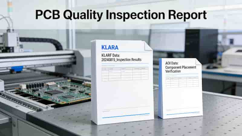
PCB Inspection and Test Files Including KLARF and AOI Data

File Specification Comparison Table

File TypePurposeRequired FormatUsage Stage
GerberLayer imagingRS-274X / X2PCB Fabrication
NC DrillHole drillingExcellonPCB Fabrication
BOMComponent listExcel / CSVPCBA Assembly
CentroidSMT placementXY Data / TXTPCBA Assembly
KLARFAOI inspectionStandard KLARFQuality Test

Conclusion

Complete and standardized PCB & PCBA manufacturing files are critical for accurate quoting, fast prototyping, consistent mass production, and high-quality assembly. Using Gerber RS-274X, proper BOM, Centroid files, and NC Drill files ensures zero rework and on-time delivery for global projects.

We support all standard PCB and PCBA file formats and provide DFM analysis to optimize your design for manufacturability.
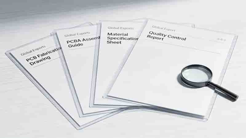
Complete PCB and PCBA Manufacturing File Package for Global Export

Ready for Your PCB & PCBA Project?

Submit your PCB & PCBA manufacturing files for a free DFM check and instant quote.

Request a Quote Now
Buried PCB via connecting inner layers only

PCB Vias Explained: Through, Blind, and Buried Holes

Posted on
0 Comments
PCB vias connect layers in multilayer circuit boards, enabling compact, high-performance electronics. This guide covers plated through holes, blind, and buried vias, their design, manufacturing, and advantages in modern PCB fabrication. From 5G devices to automotive systems, understand how to choose the right via type for your project. What Are PCB Vias? A PCB via…
SMT PCB AOI and X-ray Inspection Equipment

Surface Mount Technology (SMT) PCB Assembly Service

Posted on
0 Comments
Surface Mount Technology (SMT) PCB Assembly Service mounts electrical components directly onto the surface of printed circuit boards without through-hole leads. As a leading assembly solution for modern electronics, it delivers compact size, high reliability, and cost efficiency for industrial, medical, automotive, and consumer products worldwide. We provide one-stop service covering PCB production, component sourcing,…
PCB board after dry film lamination process

Navigating The PCB Manufacturing Process Part 2: Copper Plating, Routing

Posted on
0 Comments
In our PCB manufacturing process deep dive, we explored lamination, exposure, and development steps that transfer circuit layouts onto boards. Up next, we tackle graphical electrodeposition and AOI. PCB Copper Plating In the previous article, we covered the first and second steps of the PCB manufacturing process – MI (Manufacturing Instruction), which involves crafting a…
Laser Drilled vs Photoimageable Microvias PCB

The Essentials of Microvias – Enabling Miniaturization in PCBs

Posted on
0 Comments
As printed circuit boards pack more components into smaller spaces, microvias enable advanced PCB miniaturization for HDI PCBs. We explain core technology, fabrication, types, reliability, and industrial applications for engineers and global buyers. What Are Microvias As printed circuit boards are designed to pack ever more components into compact spaces, manufacturers use microvias to enable…
PCB dielectric strength HIPOT test equipment and process

Ultimate Guide to PCB Materials, Dielectric Strength, and Testing in 2025

Posted on
0 Comments
Dielectric strength is critical for PCB reliability, ensuring insulation and safety in high-voltage and high-frequency applications. This guide dives into key PCB materials, their dielectric properties, testing techniques, influencing factors, and practical advice for designing robust circuits. Introduction In the fast-paced world of electronics, a single oversight in PCB design can lead to catastrophic failure—like…
Rigid Flexible PCB Basic Structure Diagram

Rigid-Flex PCB Stackup: Design and Manufacturing Guide

Posted on
0 Comments
Rigid-flex PCB stackup combines rigid and flexible layers for compact, reliable designs. Explore its types, design tips, and applications in this professional guide. Introduction to Rigid-Flex PCB Rigid-flex PCBs combine the strengths of rigid and flexible circuits, creating a hybrid solution for complex, high-density electronic designs. Integrated by plated through holes (PTH), these boards support…

FAQs About PCB & PCBA Manufacturing Files

A: Core files include Gerber files, NC Drill files, native design files and stack-up documents for impedance control.

A: RS-274X and Gerber X2 are widely used. The old RS-274D is outdated and not suggested for use.

A: You need BOM list, Centroid pick-and-place file, assembly drawings and related test documents.

A: It adopts Excellon format to define hole positions, diameters and tool numbers for PCB drilling process.

A: Also called XY data, it provides component coordinates and rotation angles for automated SMT placement machines.

A: KLARF files work with AOI equipment to support automated optical inspection and quality checking for finished boards.

Similar Posts