This guide covers everything about PCB solder mask (solder resist), including its functions, types, colors, application processes, thickness standards, IPC testing, and assembly compatibility. Learn how solder mask protects circuits, prevents solder bridging, and improves reliability for industrial and high-density PCBs. We explain how to select the right solder resist for rigid, flexible, and high-speed PCB applications.
What Is Solder Mask in PCB?
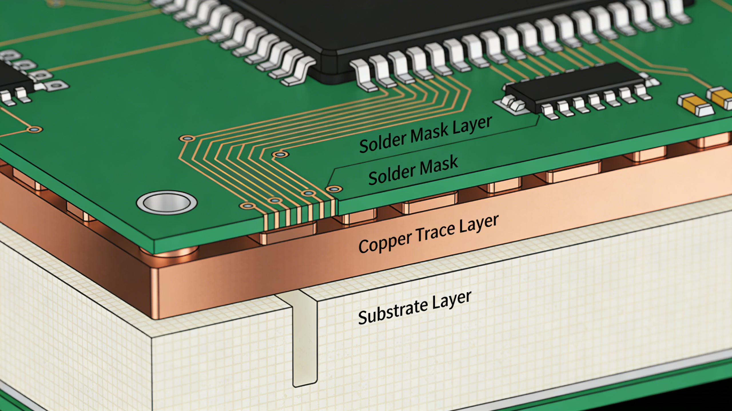
PCB solder mask — also known as solder resist or solder stop — is a protective polymeric coating applied to the surface of printed circuit boards. Its primary role is to insulate copper traces, prevent oxidation, and stop molten solder from bridging between pads during assembly.
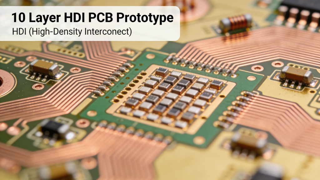
Beyond protection, solder mask improves visual inspection, supports AOI systems, and enhances chemical and mechanical resistance against moisture, dust, and abrasion. For high-density SMT and BGA designs, proper solder resist application is critical to avoid short circuits and assembly failures.
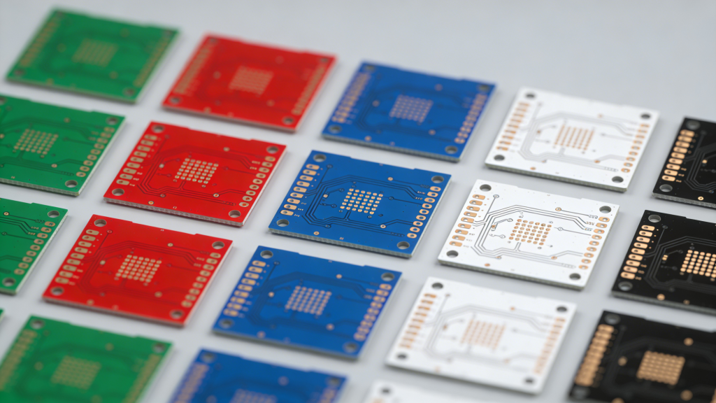
PCB Solder Mask Colors and Applications
Green remains the industry standard due to high contrast, cost stability, and military heritage. However, modern manufacturing supports multiple colors for branding, optical needs, and functional differentiation.
- Green: Best for general-purpose, inspection visibility, and mass production
- Red / Blue: High contrast with silkscreen, ideal for label-heavy designs
- White: Preferred for LED PCBs and metal-core boards to boost light reflectivity
- Black: Used for anti‑glare applications; requires careful thermal management
- Yellow / Purple / Matte: Custom options for branding and specialized devices
Main Types of PCB Solder Mask
Modern PCB production uses four primary categories of solder mask systems, each suited to different precision and cost requirements.
- Liquid Photoimageable (LPI): Most widely used for high-precision PCBs, applied via spray, curtain coat, or screen print
- Dry Film Photoimageable: High resolution for fine-pitch HDI boards
- Liquid Epoxy: Low-cost solution for simple single and double-layer boards
- Peelable Solder Mask: Temporary protection for selective areas during HASL and wave soldering
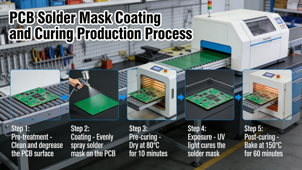
Solder Mask Application Process
A standard industrial PCB solder mask production flow follows strict steps to ensure adhesion and accuracy:
- Surface cleaning and micro-roughening for strong adhesion
- Coating via spray, curtain, or screen printing
- Pre-baking to evaporate solvents
- UV exposure and development to open pad areas
- Final thermal curing for full hardness and resistance
- Inspection against IPC standards for registration and defects
Key Solder Mask Properties & Thickness Standards
Typical solder mask thickness ranges from 15–35 μm, with 20–25 μm as the industry norm. Too thin risks copper exposure; too thick causes component tilting and poor solderability.
High-quality solder resist must offer strong thermal resistance, solvent resistance, adhesion, and insulation performance to meet IPC-SM-840C requirements.
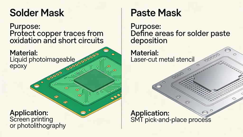
Solder Mask vs Paste Mask: Key Differences
| Item | PCB Solder Mask | Paste Mask (Stencil) |
|---|---|---|
| Purpose | Permanent protection & insulation | SMT solder paste application |
| Part of PCB | Yes, permanent layer | No, assembly tool only |
| Opening Size | Larger than pads | Equal or smaller than pads |
Solder Mask Testing & Quality Standards
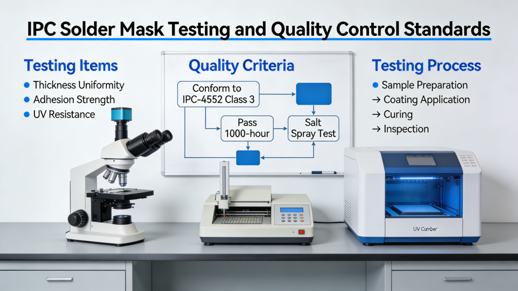
Reliable PCB solder mask production follows IPC-TM-650 and IPC-SM-840C testing standards, including:
- Adhesion tape test
- Pencil hardness test
- Thermal shock and solder heat resistance
- Acid, alkali, and solvent resistance
- Thickness measurement and registration accuracy
Conclusion
PCB solder mask is far more than a cosmetic layer — it is a critical component of long-term PCB reliability, assembly yield, and electrical performance. Choosing the right type, color, thickness, and application method directly impacts the quality of rigid, flexible, HDI, and high-speed PCBs.
Working with an experienced manufacturer ensures your solder resist meets IPC standards and performs consistently in real-world environments.
Need Custom PCB Solder Mask Solutions?
Contact us today for a free quotation, technical consultation, or custom solder mask specifications for your PCB project.
Request a Quote Now
How to Solder On Flex PCB? Complete Professional Guide

What is a Blank PCB? Buy Bare Circuit Boards | Layer PCB
What is a PCB BOM and How to Create One
Turnkey PCB Assembly Services | Full & Partial Solutions
Rigid-Flex PCB Stackup: Professional Design & Manufacturing Guide