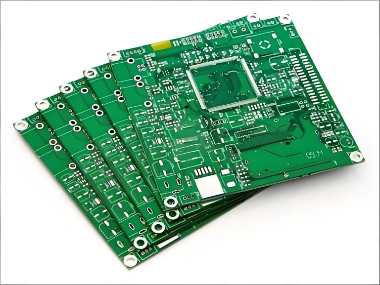
Factory-direct 4 Layer PCB with standard FR4 stackup, fast prototype lead time, free DFM support, and reliable quality for global industrial, IoT, and communication projects.
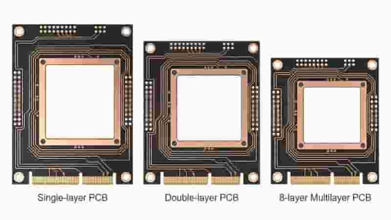
What Is a 4 Layer PCB?
A 4 Layer PCB (four‑layer printed circuit board) is a multilayer circuit board that contains four copper layers laminated together with insulating dielectric material, typically FR4.
Compared with a simple 2 layer PCB, a 4 layer board adds internal power and ground planes, which improves signal integrity, EMI performance, and power distribution in compact designs.
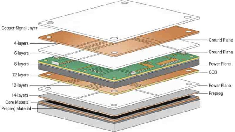
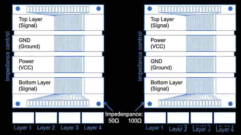
4 Layer PCB Structure and Layer Functions
In a standard 4 Layer PCB structure, the two outer layers (top and bottom) are mainly used for component placement and signal routing. The two inner layers typically act as solid planes – one for ground (GND) and one for power (VCC).
This structure provides low‑impedance return paths for high‑speed signals and helps reduce electromagnetic interference (EMI).
The 4 Layer PCB stackup offers more routing channels and better reference planes than a 2 layer PCB, while staying more cost‑effective than 6 layer or higher boards.
Standard 4 Layer PCB Stackup & Thickness
A standard 4 Layer PCB stackup balances signal integrity, EMI performance, manufacturability, and cost. The most common configuration uses outer layers for signals and inner layers for power and ground planes.
Typical 4 Layer FR4 PCB Stackup
| Layer | Function | Notes |
|---|---|---|
| Top Layer | Signal + Components | Main routing for critical signals |
| Inner Layer 1 | Ground Plane (GND) | Reference plane for return currents |
| Inner Layer 2 | Power Plane (VCC) | Stable power distribution |
| Bottom Layer | Signal + Components | Secondary routing & I/O |
Three Common 4 Layer PCB Stackup Types
1. Standard Signal‑GND‑VCC‑Signal – Best for general industrial & communication designs.
2. Power‑Inner Signal‑Inner Signal‑GND – Best for high‑speed & EMI‑sensitive applications.
3. Signal‑GND‑VCC‑Signal (Optimized) – Best for high‑density & complex layouts.
Standard 4 Layer PCB Thickness
The standard thickness of a 4 Layer PCB is 1.6 mm. Common options include 0.8 mm, 1.0 mm, 1.2 mm, and 2.4 mm for special requirements.
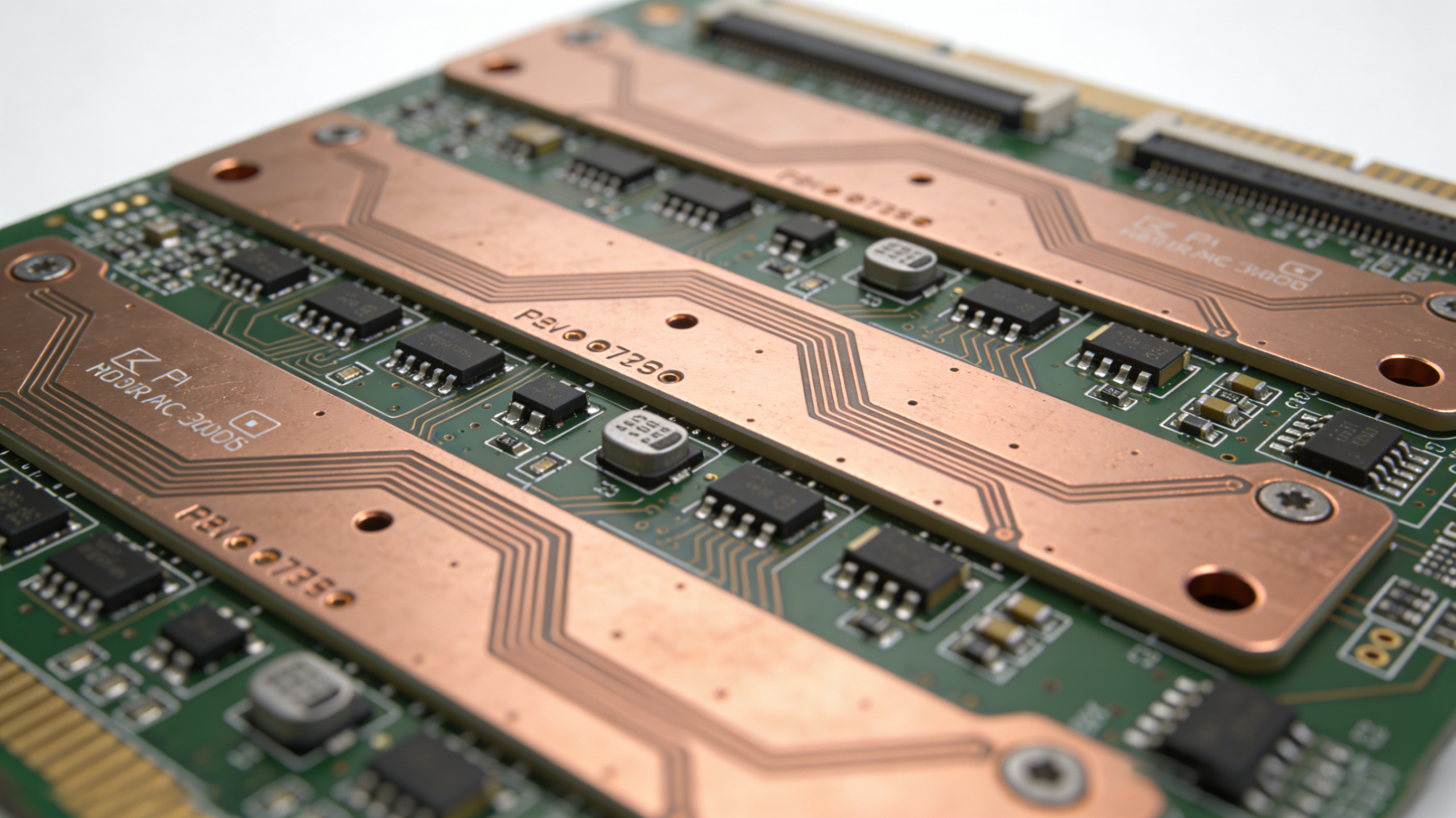
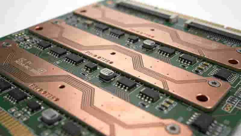
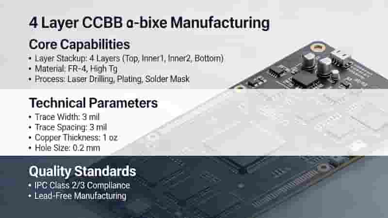
4 Layer PCB Capabilities & Specifications
We provide full‑featured manufacturing for 4 Layer PCB from prototypes to volume production, supporting standard FR4 and high‑performance materials.
| Specification | Standard Capability |
|---|---|
| Board Material | FR4 (TG130/TG150/TG170) |
| Layer Count | 4 Layer Multilayer PCB |
| Board Thickness | 0.8–2.4 mm (standard 1.6 mm) |
| Copper Weight | 0.5–3 oz (standard 1 oz) |
| Min Trace/Space | 4/4 mil or better |
| Min Finished Hole | 0.2 mm mechanical drill |
| Surface Finish | HASL, LF‑HASL, ENIG, Immersion Tin/Silver |
| Testing | 100% Electrical Test + AOI |
We also support 4 Layer PCB rigid‑flex, high‑frequency, and controlled impedance designs for advanced applications.
Advantages & Applications of 4 Layer PCBs
4 Layer PCB delivers better performance than 2 layer boards at a lower cost than 6+ layer boards, making it the most popular choice for industrial and electronic products.
Key Advantages:
- Higher routing density and smaller board size
- Improved signal integrity and reduced EMI
- Stable power delivery and better thermal performance
- Balanced cost and performance for mass production
Typical Applications:
- Industrial control & automation equipment
- Communication devices & networking modules
- IoT, consumer electronics & smart devices
- Automotive electronics & medical instruments
4 Layer PCB Price & Prototype Service
The cost of a 4 Layer PCB depends on size, quantity, materials, surface finish, and lead time. We offer factory‑direct pricing with no middleman markup.
Factors Affecting Cost:
- Board dimensions and panel utilization
- Order volume: prototype vs mass production
- Material type: standard FR4 vs high‑frequency
- Copper thickness, trace/space, and special processes
We support fast 4 Layer PCB prototypes (24–48 hours) and stable volume production with global delivery.
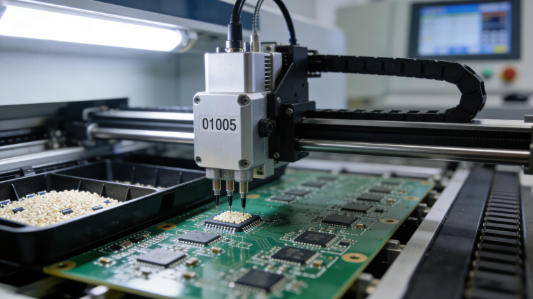
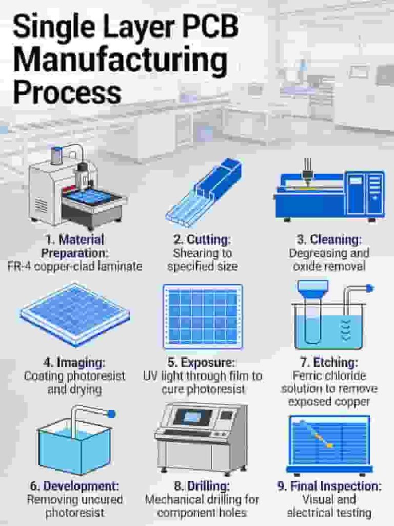
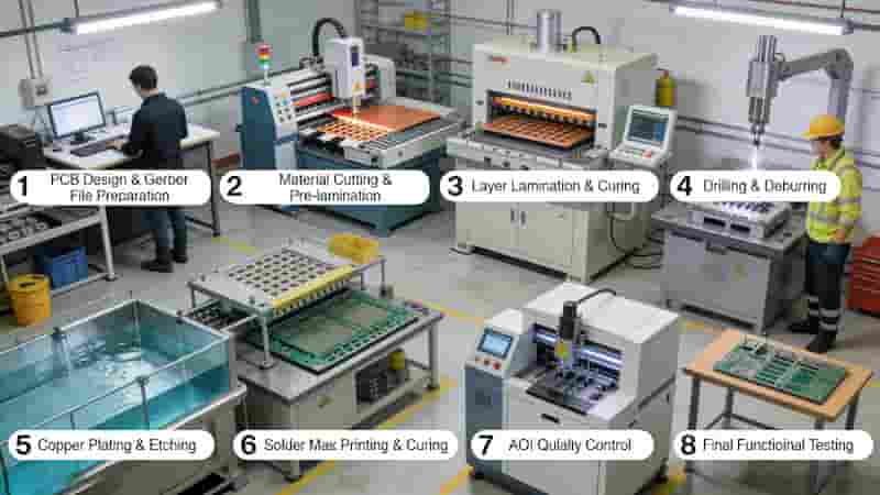
4 Layer PCB Manufacturing Process
- Inner layer imaging, etching & AOI inspection
- Black oxide treatment & multi‑layer lamination
- Precision drilling & copper plating
- Outer layer circuit formation
- Solder mask, surface finish & silkscreen
- Final electrical test & quality inspection
DFM Check & Design Support
We provide free DFM check for all 4 Layer PCB designs before production to avoid manufacturing risks, reduce costs, and shorten lead times.
Our engineers review trace/space, hole size, annular ring, stackup, impedance, and assembly compatibility to ensure your design is producible.
Why Choose Our 4 Layer PCB Service
- Factory‑direct pricing with transparent cost structure
- Fast prototype & reliable production lead time
- ISO‑standard quality control & 100% testing
- Free DFM review & professional engineering support
- Global export service with on‑time delivery
Summary
Our factory‑direct 4 Layer PCB manufacturing and prototype service provides high quality, fast lead times, competitive pricing, and free DFM support for global industrial buyers, engineers, and procurement teams.
Start Your 4 Layer PCB Project Today
Upload your Gerber files for a free DFM check and get an instant quote.
Get Instant 4 Layer PCB Quote | Free DFM Check | Global Delivery
Factory‑direct 4 layer PCB manufacturing with competitive pricing, fast turnaround, and professional DFM support for global customers.