PCB stackup design directly determines signal integrity, EMI control, power stability and manufacturing reliability. This guideline provides professional, field-proven best practices for 2‑layer PCB stackup, 4‑layer PCB stackup and 6‑layer PCB stackup for industrial electronics, communications equipment and high‑speed digital products.
Introduction to PCB Stackup Design
PCB stackup design is the foundation of high‑performance printed circuit board development. It affects impedance control, electromagnetic interference (EMI), thermal management, structural strength and production cost. A well‑designed layer stackup ensures stable signal transmission, efficient power delivery and high yield in mass production.
Whether you are designing low‑frequency analog circuits or high‑speed digital systems, standardized PCB stackup design helps balance performance, cost and manufacturability.
Key Rules for PCB Stackup Design
All reliable PCB stackup design follows two non‑negotiable core principles:
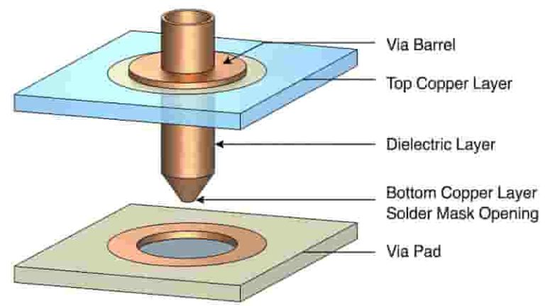
- Adjacent Reference Layer: Every signal layer must have an adjacent ground or power plane to provide a short signal return path and suppress EMI effectively.
- Minimize Power‑Ground Spacing: Place power planes and ground planes closely to increase coupling capacitance, filter high‑frequency noise and improve power integrity.
2‑Layer PCB Stackup Design
2‑layer PCBs are cost‑effective and widely used in low‑frequency applications below 10 kHz. Proper PCB stackup design reduces EMI and improves stability.
- Use radial power routing to reduce loop area and inductance
- Route ground traces adjacent to critical signal paths
- Use wide ground paths on the opposite side of key signals
- Avoid long parallel runs to minimize crosstalk
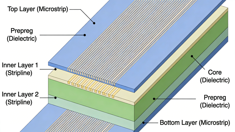
4‑Layer PCB Stackup Best Practices
4‑layer PCBs deliver the best balance of performance and cost. Below are industry‑standard PCB stackup design architectures.
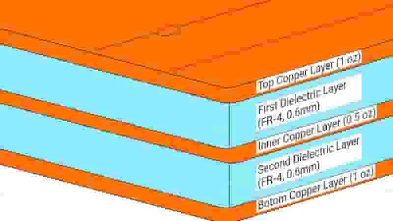
Structure 1: SIG – GND – PWR – SIG
- Good signal integrity for high‑density components
- Suitable for digital circuits with moderate speed
- Widely used in consumer and industrial electronics
Structure 2: GND – SIG – SIG – GND
- Excellent EMI shielding with outer ground layers
- Ideal for noise‑sensitive analog and mixed‑signal systems
- Preferred for automotive and medical devices
Design Tips: Follow the 20H rule, control impedance, and cross‑layer routing vertically.
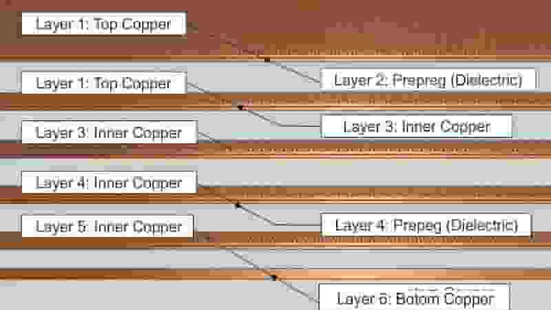
6‑Layer PCB Stackup for High‑Speed Designs
6‑layer PCB stackup design supports high‑clock‑frequency circuits and high‑density layouts with strict SI and EMI requirements.
Structure 1: SIG – GND – SIG – PWR – GND – SIG
- Each signal layer has a nearby ground reference
- Excellent for high‑speed signal integrity
- Widely used in networking, computing and FPGA designs
Structure 2: GND – SIG – GND – PWR – SIG – GND
- Superior EMI shielding with full ground planes
- Best for high‑noise environments and military‑grade products
- Higher cost but maximum reliability
Advanced PCB Stackup Optimization Tips
- Use simulation tools for controlled impedance calculation
- Tighten power‑ground pairs to enhance noise filtering
- Balance layer count between cost and performance
- Follow DFM rules to ensure high production yield
- Use consistent dielectric thickness for stable impedance
PCB Stackup Comparison: 2‑Layer vs 4‑Layer vs 6‑Layer
| Item | 2‑Layer PCB | 4‑Layer PCB | 6‑Layer PCB |
|---|---|---|---|
| Cost | Lowest | Medium | Higher |
| EMI Performance | Basic | Good | Excellent |
| High‑Speed Support | No | Moderate | Yes |
| Typical Use | Low‑freq devices | General industrial | High‑speed systems |
Frequently Asked Questions (FAQ)
What is the best PCB stackup for EMI control?
The GND‑SIG‑SIG‑GND 4‑layer stackup and GND‑SIG‑GND‑PWR‑SIG‑GND 6‑layer stackup provide the strongest EMI shielding.
How to choose between 4‑layer and 6‑layer PCB?
Choose 4‑layer for cost‑effective general designs; choose 6‑layer for high‑speed, high‑density or noise‑critical applications.
How to reduce EMI in PCB stackup design?
Use adjacent reference planes, tight power‑ground coupling, and controlled impedance routing.
What tools are used for PCB stackup design?
Altium Designer, Cadence Allegro, KiCad and Polar SI9000 are widely used for stackup simulation and impedance calculation.
Conclusion
Standardized PCB stackup design is critical for achieving reliable, high‑performance and cost‑efficient PCBs. Following these guidelines for 2, 4 and 6‑layer boards helps optimize signal integrity, reduce EMI and improve manufacturing yield.
Get Professional PCB Stackup & Manufacturing Support
Need custom PCB stackup design, DFM review, prototyping or mass production? Our engineering team provides free stackup suggestions and competitive quotes for 2‑layer, 4‑layer and 6‑layer PCBs.
Request Stackup Advice & Quote
What Is Prototype PCB Assembly
Step Stencil Manufacturing | Precision Multi-Level SMT Stencils
Key Factors Influencing Custom PCB Costs in 2025
High Tg PCB Manufacturing for High Temperature Applications