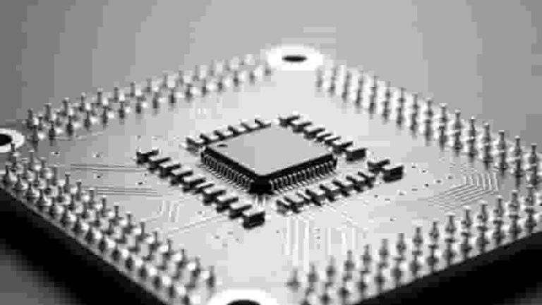
Fast Prototype PCB Manufacturing Services in Canada 

PCB Materials Surface Finishes Prototype Manufacturing Canada

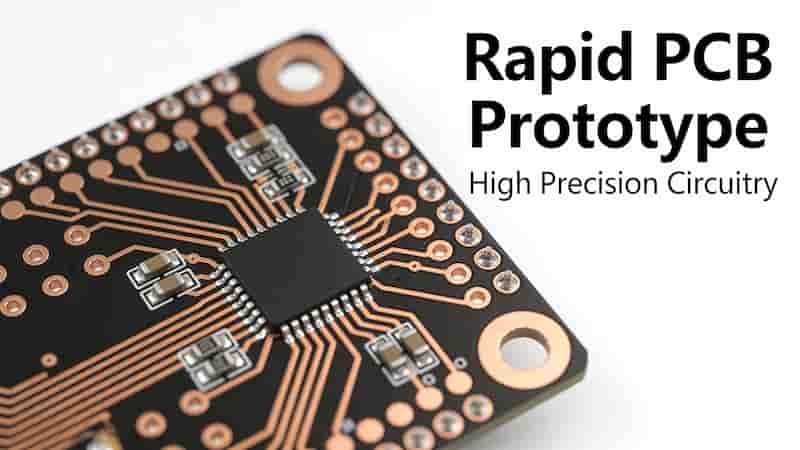
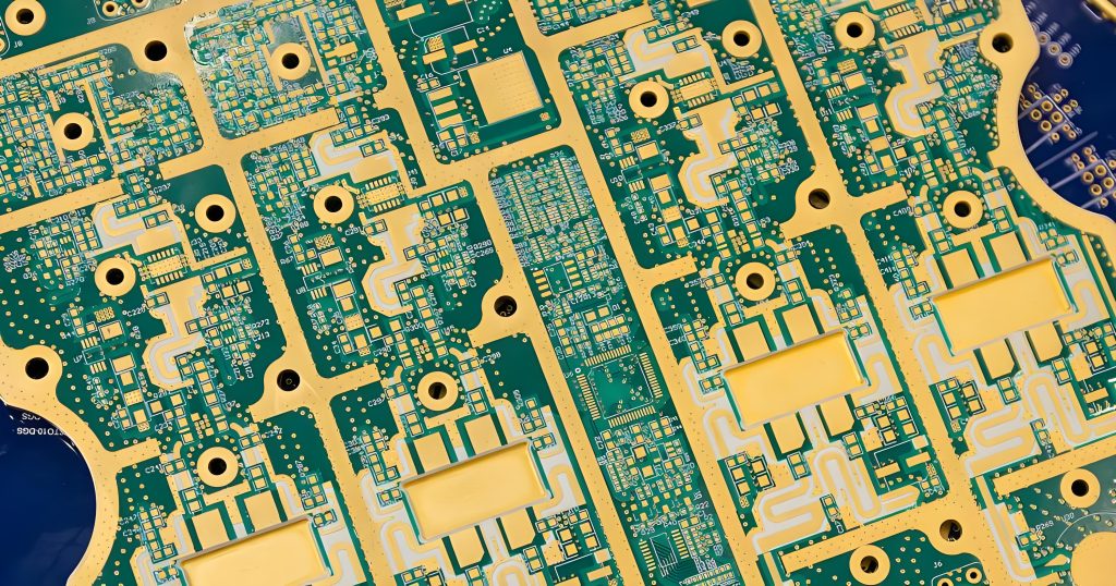
Fast Prototype PCB Manufacturing Services in Canada provide rapid, high‑reliability printed circuit board prototyping for engineers, procurement teams, and OEMs across Canada. We offer quick‑turn rigid, flexible, rigid‑flex, HDI, and high‑frequency PCBs with IPC Class 2/3 standards, DFM support, 48–72 hour lead times, and seamless scaling to volume production.

Core Prototyping Capabilities

Our fast prototype PCB manufacturing supports full‑range specifications to meet Canadian product development demands.

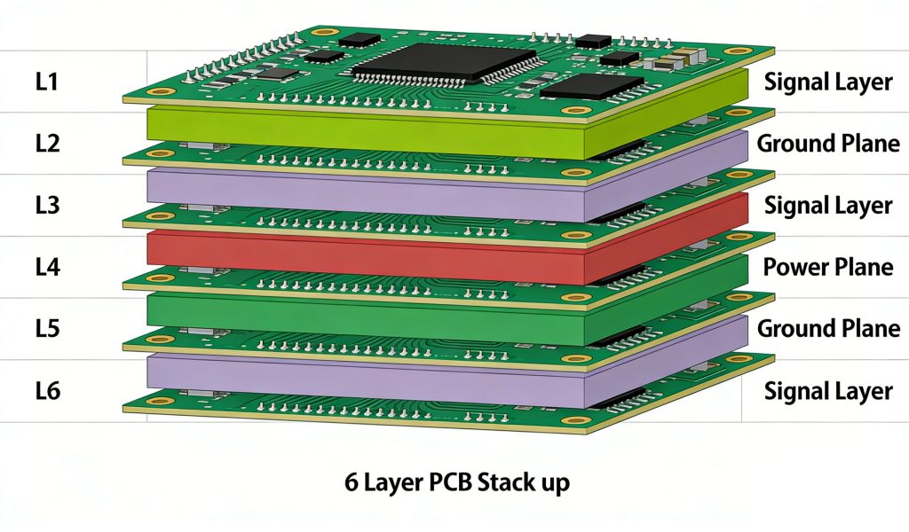
  • Layer count: 1–64 layers (single‑sided, double‑sided, multilayer, HDI)
  • Board thickness: 0.4mm–3.2mm
  • Max size: 24×24 inches
  • Minimum order: 5 pieces
  • Lead time: 48–72 hours for standard designs
  • Full electrical testing & AOI inspection
  • Optional SMT assembly & turnkey solutions

PCB Prototype Capabilities Canada Fast Prototype Manufacturing

Materials & Surface Finishes

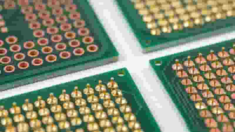
We use certified materials for prototype PCB manufacturing compatible with industrial, automotive, and IoT applications in Canada.

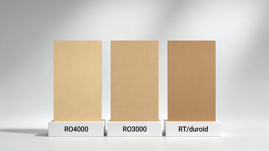
  • Base materials: FR‑4, High‑Tg FR‑4, Rogers, PTFE, aluminum, copper core
  • Surface finishes: HASL, lead‑free HASL, immersion gold, ENIG, immersion silver, immersion tin
  • Special types: flexible PCB, rigid‑flex PCB, metal core PCB, high‑frequency PCB
PCB Materials Surface Finishes Prototype Manufacturing Canada

Quality & Industry Standards

Our fast prototype PCB services follow strict international standards to ensure reliability for Canadian clients.

  • ISO 9001 & IATF 16949 certified
  • IPC‑A‑600 Class 2 / Class 3 compliance
  • 100% electrical test before shipment
  • Full DFM analysis free of charge
  • RoHS & REACH compliant materials

Advantages for Canadian Customers

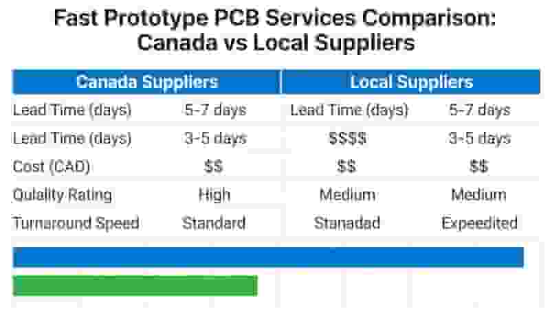
We deliver better value for prototype PCB in Canada compared to local suppliers.

ItemOur ServicesLocal Canadian Suppliers
Lead Time48–72 hours7–10+ days
Cost50–60% lowerHigher
Material OptionsFull rangeLimited
DFM SupportFreePaid or limited
  • Speed: Accelerate product development cycles
  • Cost: Lower prototype expenses without losing quality
  • Flexibility: Wide material and customization choices
  • Scalability: Smoothly move from prototype to mass production
  • Shipping: Reliable delivery via DHL / FedEx to Canada in 3–5 days
Fast Prototype PCB Advantages Canada Compared to Local

Design & Ordering Guide

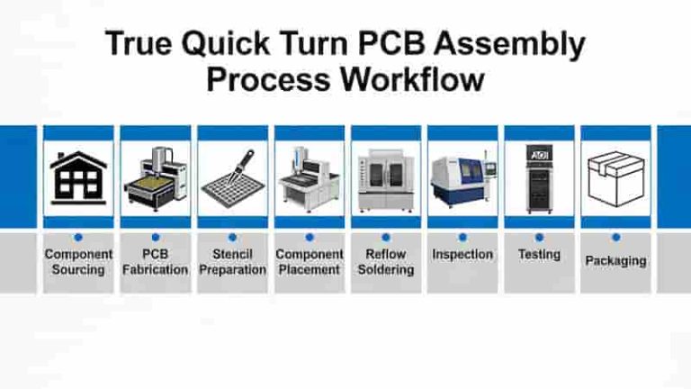
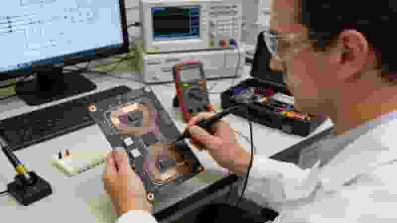
Streamline your fast prototype PCB manufacturing process with our simple workflow.

  1. Prepare Gerber files, BOM, and stackup requirements
  2. Submit files for a free DFM check and instant quote
  3. Confirm design and place order
  4. Manufacturing and full testing (48–72 hours)
  5. Express shipping to your address in Canada
Fast Prototype PCB Order Process Canada Workflow

Frequently Asked Questions

Q: How fast can you deliver prototype PCBs to Canada?
A: Standard fast prototype PCB manufacturing lead time is 48–72 hours, plus 3–5 days shipping to Canada.

Q: What is the minimum order quantity?
A: We accept orders starting from 5 pieces for prototype PCB in Canada.

Q: Do you provide free DFM analysis?
A: Yes, we offer free DFM checks to optimize your design for prototype PCB manufacturing.

Q: Can you handle flexible and rigid‑flex PCBs?
A: Yes, we support flexible, rigid‑flex, HDI, and high‑frequency prototypes for Canadian clients.

Conclusion

Our fast prototype PCB manufacturing services in Canada combine speed, quality, and cost efficiency to support product developers across industries. With short lead times, international certifications, full material options, and professional engineering support, we are a trusted partner for your PCB prototyping needs.

Get Your Fast PCB Prototype Quote Today

Send your Gerber files for a free quote and DFM analysis. We support fast prototype PCB manufacturing for all Canadian projects.

Request a Quote

Selective Wave Soldering Machine for PCB Assembly Process

Selective Wave Soldering Guidelines: Process, Parameters & Best Practices for PCB Assembly

Selective wave soldering is a precision soldering method designed for mixed-technology PCBs, protecting heat-sensitive components while delivering reliable through-hole solder joints. This professional guide covers core principles, process flow, critical parameters, DFM rules, defect resolution, and quality control for industrial PCB manufacturing. 1. Overview of Selective Wave Soldering The two primary process technologies in PCB…
Step-Up vs Step-Down Stencil for PCB SMT

Step Stencil Manufacturing | Precision Multi-Level SMT Stencils

Step Stencil Manufacturing provides precision-engineered multi-level thickness stencils for advanced PCB assembly, delivering controlled solder paste deposition for mixed-component boards and high-yield SMT production. What Is a Step Stencil A Step Stencil (multi-level stencil) is a precision SMT assembly tool designed to apply controlled solder paste volumes to PCB surfaces. Unlike standard uniform-thickness stencils, step…
HDI PCB Microvia Types: Blind, Buried, Stacked Vias

HDI PCB Layout and Basic HDI Design Guidelines

HDI PCB is an advanced printed circuit board technology for high‑component‑density electronics. This guide covers core HDI PCB layout principles, via design, trace rules, stackup, and IPC standards for engineers and buyers. What Is HDI PCB Layout? High Density Interconnects (HDI PCB) layout refers to advanced PCB design techniques used when trace widths drop below…
PCB Solder Mask full color options green red blue white black matte

PCB Solder Mask: The Complete Technical Guide for Global Buyers

PCB Solder Mask (also known as solder resist) is a protective polymer layer applied to printed circuit boards to prevent solder bridging, resist oxidation, improve insulation, and ensure long‑term reliability in SMT assembly and industrial applications. This guide covers definitions, types, colors, processes, DFM rules, IPC standards, testing, and troubleshooting for engineering and procurement teams…
High TG PCB laminate structure and glass transition temperature diagram

High TG PCB Material: Thermal Stability, Key Benefits, Industrial Applications & Professional Fabrication Solutions

High TG PCB Material: The Ultimate Guide to High-Reliability Circuit Boards High TG PCB material (Tg ≥170°C) delivers superior thermal stability, low Z‑axis CTE, and long‑term reliability for high‑power, high‑temperature, and high‑density electronic systems. This guide covers core advantages, industry applications, material types, fabrication controls, and how we support your custom High TG PCB projects…
Blind Via Structure in Multilayer PCB HDI Design

Blind Vias & Buried Vias in PCBs – The Complete Engineering Guide

Blind vias and buried vias are core structures for high‑density interconnect (HDI) and high‑speed PCBs. They boost routing density, signal integrity, and miniaturization while optimizing layer stackups. This guide covers definitions, differences, design rules, manufacturing, and industrial applications for global engineers and buyers. Introduction As printed circuit boards become more compact and integrated, advanced via…

Similar Posts