Our advanced flex PCBprototyping delivers flexible, lightweight, and reliable flexible circuits for innovative electronics designs. Enjoy rapid turnaround and full engineering support.
What Is Flex PCB
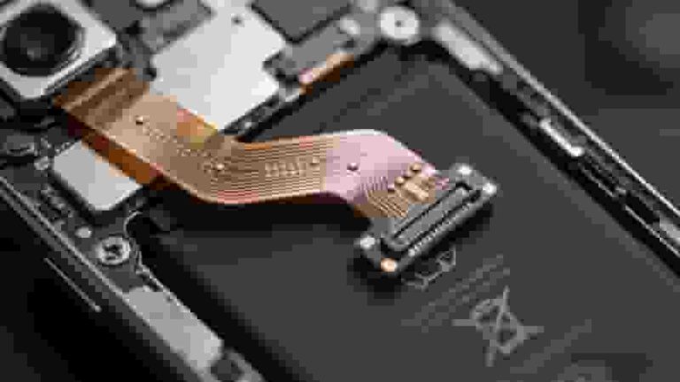
Flex PCBs are essential components in modern electronics including mobile devices, desktop printers, and hard drives. Built with a flexible substrate with or without coverlay, flexible PCBs integrate complex circuitry in a bendable form factor.
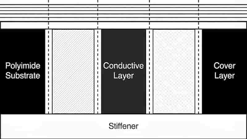
Made from PET (Polyester) or polyimide, flex PCBs deliver superior flexibility and long‑term reliability for compact, high‑performance electronic products.
Advanced flex PCB technology encourages brands to build prototypes before mass production, helping detect design flaws early and avoid costly production mistakes.
What Is Flex PCB Prototyping
Flex PCB prototyping is the process of manufacturing small‑batch flexible printed circuit boards to validate, test, and refine designs before volume production.
Using polyimide or PET substrates, flex PCB prototypes offer outstanding flexibility, lightweight build, and durability ideal for wearables, medical devices, automotive systems, and consumer electronics.
Key Benefits of Flex PCB Prototyping
- Lightweight Design: Polyimide‑based flex PCBs are much lighter than FR4 boards, enabling ultra‑compact devices.
- Superior Flexibility: Supports bending, twisting, and 3D routing to fit tight spaces and reduce assembly size.
- Ultra‑Thin Profile: 2‑layer flex PCB prototypes measure just 4.4–10 mils, perfect for miniaturization.
- High-Temperature Resistance: Stable in extreme heat, oils, gases, and corrosive environments.
- Cost Efficiency: Catches design errors early to lower mass production risks and expenses.
- Excellent Signal Integrity: High circuit density with minimal wiring errors.
- Strong Durability: Fewer interconnects improve shock resistance and performance under dynamic stress.
Applications of Flex PCB Prototyping
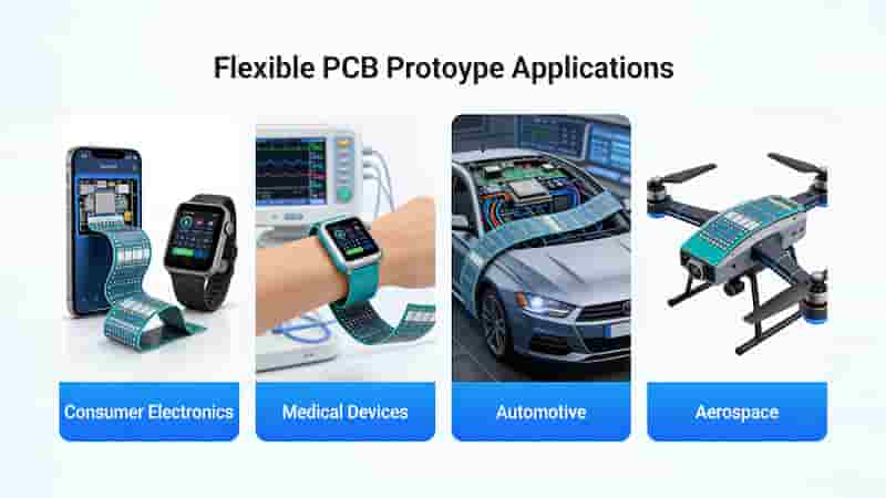
Flex PCB prototypes drive innovation across key industries:
- Consumer Electronics: Smartphones, smartwatches, flexible displays
- Medical Devices: Biocompatible circuits for diagnostics and wearable health tools
- Automotive: Sensors and control units in space‑constrained vehicle systems
- Aerospace: Lightweight, high‑reliability circuits for avionics and satellites
- Industrial: Robust boards for automation and control equipment
- Military & Communications: High‑performance circuits for secure, compact systems
Flex PCB Classifications
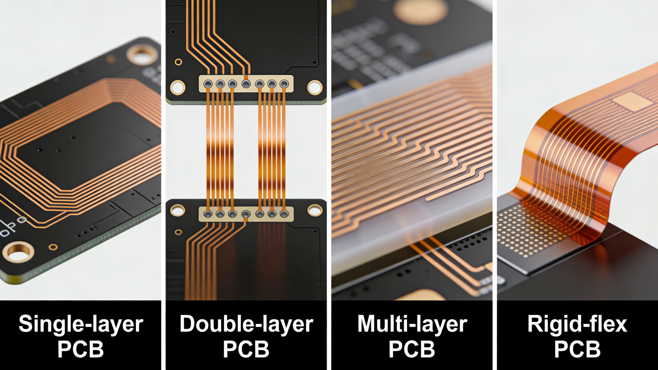
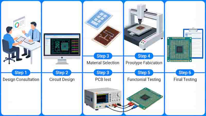
Single Layer Flex PCB
Single conductive layer on flexible substrates (polyimide / PET). Cost-effective for simple circuits. Used in basic consumer electronics.
Double-sided Flex PCB
Conductive patterns on both sides connected by plated vias. Improves layout flexibility and component density. Ideal for wearables and medical devices.
Multilayer Flex PCB
Three or more laminated layers with interlayer connections. Boosts reliability, thermal management, and assembly performance. Used in aerospace and industrial systems.
Rigid-flex PCB
Combines flexible and rigid layers for stable, space‑saving 3D designs. Reduces connectors and enhances reliability. Applied in automotive, military, and high‑reliability products.Flex PCB Type Comparison
Flex PCB Type Comparison
| Type | Layers | Key Feature | Typical Applications |
|---|---|---|---|
| Single Layer | 1 | Low cost, simple circuit | Basic consumer electronics |
| Double-sided | 2 | Plated vias for interlayer connection | Wearables, medical devices |
| Multilayer | 3+ | High density, thermal management | Aerospace, industrial systems |
| Rigid-flex | Mixed | Combines rigid and flexible sections | Automotive, military, high-reliability |
Flex PCB Prototyping Process
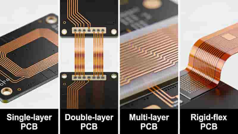
Our streamlined flex PCB prototyping workflow ensures precision and consistency:
Prototyping Workflow Overview
| Step | Process | Key Activity | Output |
|---|---|---|---|
| 1 | Design Consultation & DFM | Optimize design for manufacturability | DFM report |
| 2 | Material Selection | Choose polyimide, PET, adhesive cores | Material specification |
| 3 | Stackup Design | Define layers, thickness, coverlays | Stackup diagram |
| 4 | Prototyping | Advanced production run | Prototype boards |
| 5 | Testing & Validation | Electrical and mechanical checks | Test report |
| 6 | Feedback & Iteration | Refine for mass production | Final design files |
Why Choose Our Flex PCB Prototyping
- Proven Expertise: Years of experience in flex PCB manufacturing and prototyping
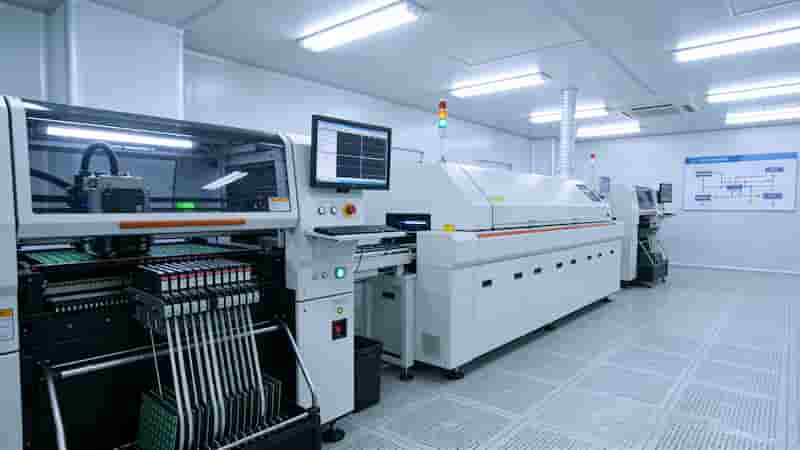
- Advanced Equipment: High‑precision machinery for consistent quality
- Full Service Coverage: From prototyping to PCB assembly and component sourcing
- Fast Turnaround: 24‑hour rapid prototype options available
- No MOQ Limit: Support for startups and large‑scale projects
- Cost Effective: Competitive pricing with free DFM analysis
- Global Customer Support: Professional service for international buyers
Flex PCB Prototyping Pricing Factors
Cost of flex PCB prototyping depends on these key elements:
Cost Breakdown by Factor
| Factor | Impact | Description |
|---|---|---|
| Board Size | Per square inch | Larger boards increase material and processing cost |
| Layer Count | 1.5–2x per added layer | Double-sided and multilayer cost more than single-layer |
| Order Volume | Low volume adds tooling | Efficient processes minimize setup costs |
| Materials | Varies by type | Polyimide, special coverlays, stiffeners affect price |
| Turnaround Time | Small premium for rush | Expedited 24-hour service available |
For an exact quote, send your Gerber files and BOM to our support team.
Flex PCB Manufacturing Process
- Material Preparation: Chemical cleaning for strong photoresist adhesion
- Circuit Patterning: Photoresist application and precision etching
- Lamination: Bond coverlays and solder masks securely
- Drilling & Plating: Create reliable vias for double-sided and multilayer designs
- Testing: Electrical, thermal, and mechanical performance verification
- Finishing: Add stiffeners, EMI shielding, or adhesives as required
Start Your Flex PCB Prototype Today
Turn your innovative designs into reliable products with our professional flex PCB prototyping services.
Request a Free Quote | Custom Flex PCB Prototype