This guide covers PCB drilling types, methods, workflow, parameters, quality control, DFM tips and inspection standards for engineers, buyers and manufacturers worldwide.
Introduction to PCB Drilling
PCB drilling is one of the most critical steps in printed circuit board fabrication. It creates precision holes for component mounting, layer interconnection, mechanical fixing and signal transmission. The quality of drilling directly determines PCB reliability, yield and performance.
This complete guide covers all essential knowledge of PCB drilling for global engineers, purchasers and manufacturers, including hole types, processing methods, parameters, quality standards and DFM optimization.
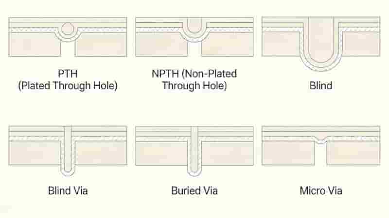
Types of PCB Holes
Different holes serve electrical and mechanical functions. Below are the most common types used in PCB drilling:
- Plated Through Holes (PTH): Conductive holes connecting all layers for component pins and layer conduction.
- Non‑Plated Through Holes (NPTH): Mechanical holes for screws, spacers and assembly fixing.
- Blind & Buried Vias: Used in HDI boards; blind vias connect outer to inner layers, buried vias inside layers only.
- Micro Vias: Holes ≤150μm, made by laser drilling for high‑density interconnects.
- Backdrilled Holes: Remove excess stub to improve high‑frequency signal integrity.
- Via‑in‑Pad: Vias inside component pads for miniaturization and thermal management.
- Half‑Holes (Castellated Holes): For board‑to‑board soldering and module connection.
- Thermal Vias: Transfer heat from power components to inner or bottom layers.
PCB Drilling Methods & Technologies
Three main methods are used in industrial PCB drilling:
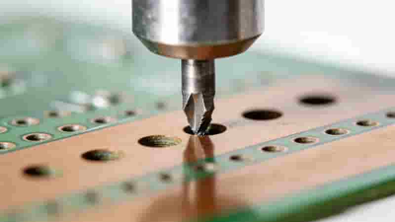
CNC Mechanical Drilling
High efficiency, low cost, suitable for mass production. Supports multi‑spindle simultaneous drilling. Limited for micro holes.
Laser Drilling
For micro vias down to 50μm, no mechanical stress, high precision. Ideal for HDI and thin PCBs.
Manual Drilling
For prototypes and small batches, flexible but dependent on operator skill.
Preparation Before PCB Drilling
Stable preparation ensures high accuracy and reduces drill breakage:
- Material selection: FR‑4, Rogers, polyimide affect drilling parameters.
- Drill files & drawings: Define hole size, position, tolerance and sequence.
- Fixture setup: Backup plates, alignment fiducials, clamping to avoid shifting.
- Tool preparation: Select drill bits, spindle speed, feed rate and coolant.
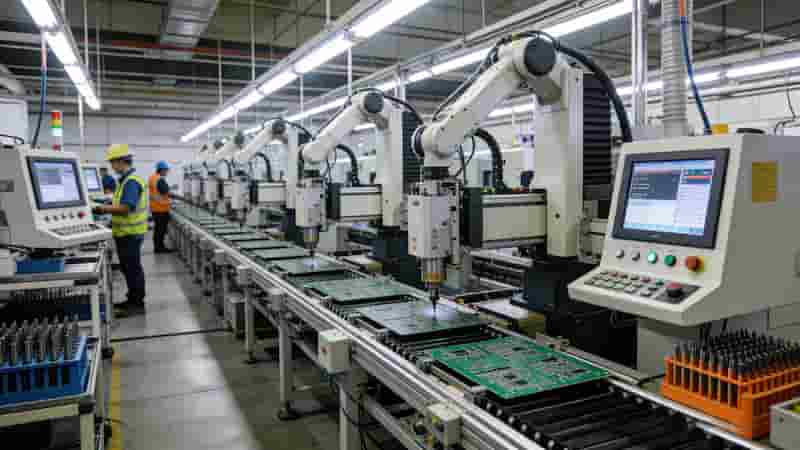
Complete PCB Drilling Workflow
- Machine cleaning and fixture installation
- Board stacking and alignment with fiducials
- Drill bit installation and parameter setting
- Auto‑alignment and first hole calibration
- Automatic drilling in programmed order
- Breakthrough detection to prevent burrs
- AOI inspection for position, size and quality
Drill Tool Selection for PCB Drilling
Key factors for choosing drill tools:
- Hole diameter matches design requirements
- Aspect ratio ≤10:1 for standard PTH
- Board thickness and material hardness
- Tolerance: ±10μm for industrial standard
- Cooling and chip removal performance
PCB Drilling Quality Control & Standards
International standards for drilling quality:
- Hole diameter tolerance: ±10μm
- Perpendicularity: ≥89°
- Position accuracy: ±20μm (high precision)
- No burrs, smearing, cracking or hole wall damage
- Plating coverage uniform for PTH
Inspection methods: AOI, CMM, cross‑section microscopy, electrical testing.
DFM Tips for PCB Drilling Designers
- Limit aspect ratio to avoid drill breakage and plating issues
- Minimize drill size types to reduce tool changes
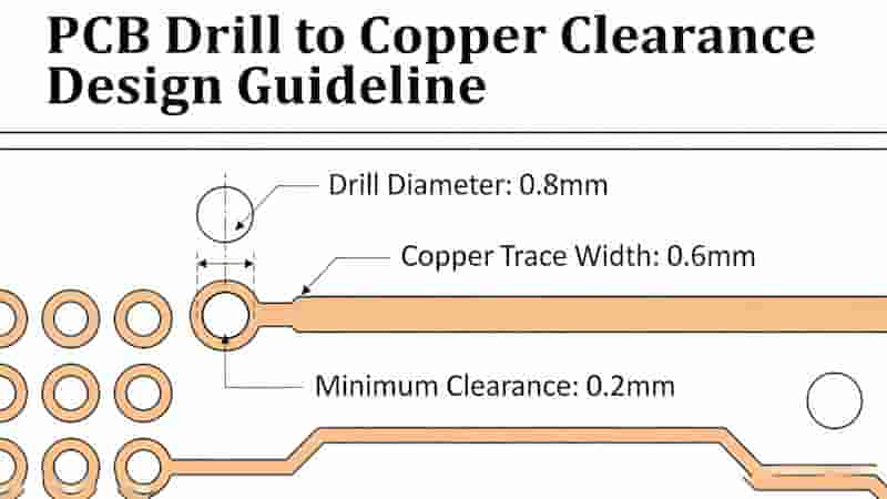
- Keep drill‑to‑copper clearance ≥8–12mil
- Mark PTH/NPTH clearly in drill files
- Avoid dense holes in small areas to prevent breakage
Mechanical vs Laser PCB Drilling Comparison
| Item | Mechanical Drilling | Laser Drilling |
|---|---|---|
| Hole Size | ≥0.1mm | ≥0.05mm (micro vias) |
| Efficiency | High (mass production) | Medium (HDI only) |
| Stress | Mechanical stress | No mechanical stress |
| Cost | Low | High |
Conclusion
PCB drilling is a core process affecting PCB quality and reliability. Mastering hole types, processing methods, parameters and quality control helps manufacturers improve yield, and helps designers create more manufacturable and stable products.
With professional PCB drilling technology and strict quality management, we support global buyers with high‑precision PCB manufacturing services for various industries.
Inquiry & Custom PCB Service
If you need professional PCB drilling support, custom PCB fabrication, quotation or DFM review, please contact us now.
We provide full‑process PCB manufacturing solutions for global importers, engineers and procurement teams.
Contact us for free quote and technical support today!