In our PCB manufacturing process deep dive, we explored lamination, exposure, and development steps that transfer circuit layouts onto boards. Up next, we tackle graphical electrodeposition and AOI.
PCB Copper Plating
In the previous article, we covered the first and second steps of the PCB manufacturing process – MI (Manufacturing Instruction), which involves crafting a manufacturing instruction document tailored to the specifics of the customer’s PCB files, and drilling. This manufacturing instruction document serves as the guiding beacon for subsequent manufacturing processes. Drilling then punctures holes in the PCB according to the design to allow different layers to connect.
Now we build upon that foundation. Copper plating chemically deposits a thin layer of copper over the entire PCB surface, including the walls of the recently drilled holes. This forms the conductive traces that carry electricity. Routing then selectively removes excess copper to leave only the desired circuit pattern.
Step 3: Plated Through Hole (PTH)
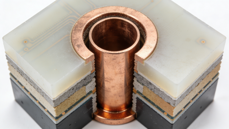
Fresh from the drilling process, the board is now dotted with holes. However, these voids are non-conductive as the walls are devoid of copper. The next critical step—copper plating, also called electroless plating, plated through hole (PTH), panel plating—deposits a thin conductive film, preparing the way for subsequent electroplating operations where copper and tin implant the tracings.
In a nutshell, copper plating fulfills two key functions:
- Coats all surfaces, including freshly minted hole walls, with a slim layer of conductive material
- Primes the board for graphical electrodeposition processes to embed circuitry
The copper plating production track is alternatively called the “conductive adhesive route.”
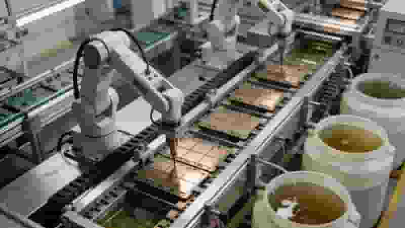
Figure 3-1. Two Fully Automated PTH Lines
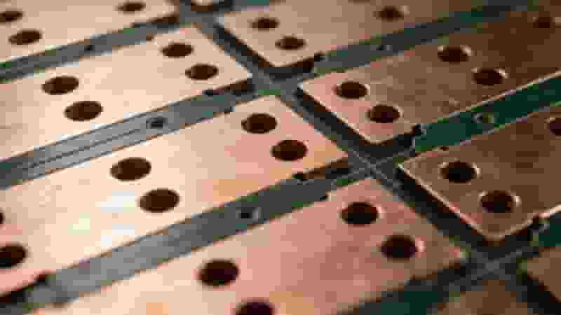
Figure 3-2. Drilled copper-clad laminate boards waiting for plating
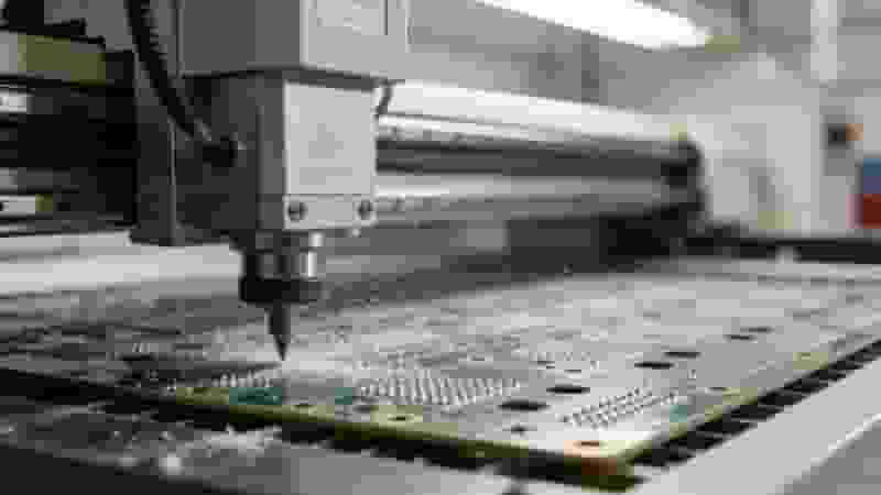
Figure 3-4. Boards passing through deburring machine
After deburring, the remaining process chain consists of chemical reactions. The key stages involve micro-etching, desmear, oxidation, polymerization, drying, and intermittent rinses.
- Micro-etching: Cleans surface oxide, removes grime, improves adhesion
- Desmear: Cleans hole walls and enhances conductivity
- Oxidation: Reacts with resin to form chemical film
- Polymerization: Deposits conductive polymer on hole walls
Post-copper plating, boards appear similar to their post-drilling state, albeit now with a conductive inner layer lining holes. Freshly plated panels bypass directly to the next process: routing.
Step 4: PCB Routing
The PCB routing process consists of three key steps in sequence: lamination, exposure, and development. Upon completion, the copper clad laminate will exhibit clearly defined circuitry.
Lamination
In PCB fabrication, the terms “dry film” and “wet film” refer to this lamination process. Compared to wet lamination, dry film delivers higher consistency and quality. We utilize the dry process.
Lamination applies an azure photosensitive film on both sides of the copper clad laminate. Post-lamination boards carry a temporary blue photoresist layer for circuit imaging.
Figure 4-1. Post-lamination boards with dry film
Exposure
We currently utilize two exposure systems: a film-based automated machine and an LDI fully automated direct imager.
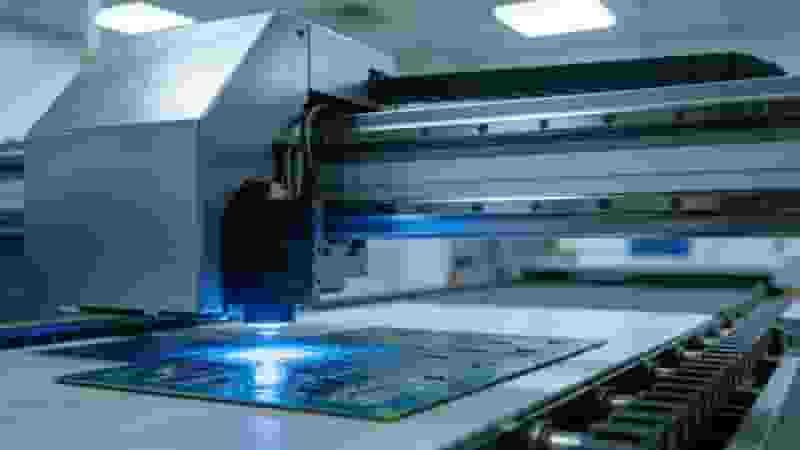
Figure 4-4. LDI laser direct imaging machine
Film-based exposure supports high-volume production, while LDI direct imaging eliminates film and suits prototyping and high-precision runs.
Development
Exposure enables subsequent development steps. Developer solution removes unexposed dry film, stripping away masked circuit regions to reveal copper beneath. The PCB routing process concludes here, ready for pattern plating.
Exposure Technology Comparison
| Parameter | Film-Based Exposure | LDI Direct Imaging |
|---|---|---|
| Production Speed | High | Medium |
| Precision | Good | Excellent |
| Best Use Case | Mass Production | Prototypes & High-Mix |
Summary
Copper plating and PCB routing are core stages that turn drilled panels into functional circuit boards. PTH creates conductivity in vias, while routing defines the exact circuit pattern via lamination, exposure, and development. These steps directly determine PCB reliability, conductivity, and production yield.
In our forthcoming installment, we will explore the fifth and sixth stages – plating circuitry through graphical electrodeposition followed by automated optical inspection.
Need Professional PCB Manufacturing Support?
Get reliable copper plating and precision PCB routing for your prototype or mass production PCB projects. We provide DFM analysis, fast lead times, and full quality control.
Request Free Quote
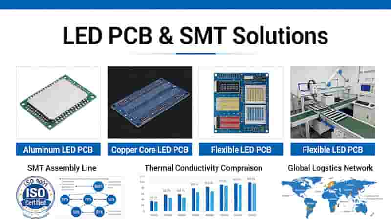
Aluminum, Copper & Flexible LED Circuit Boards with Superior Heat Dissipation
Surface Mount Technology (SMT): Advantages, Limitations & Applications
PCB Classification Guide: Types, Applications & Selection for Beginners & Pros
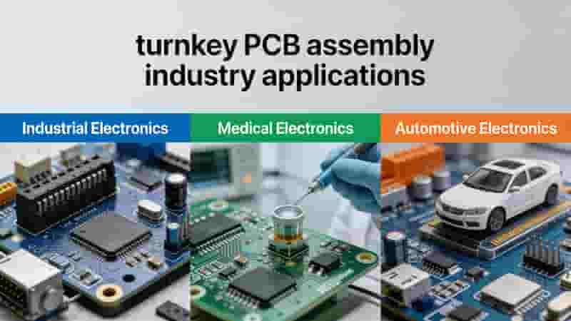
Turnkey PCB Assembly Services | Full & Partial Solutions
Prototype PCB Assembly Service – Fast, Reliable & Turnkey Solutions