Understanding the key differences between PTH and via is essential for optimizing PCB design and manufacturing. This article defines PTH and via, compares dimensions, functions, locations and finishing requirements. Typical applications and design considerations are also discussed.
Defining PTH and Vias in PCBs
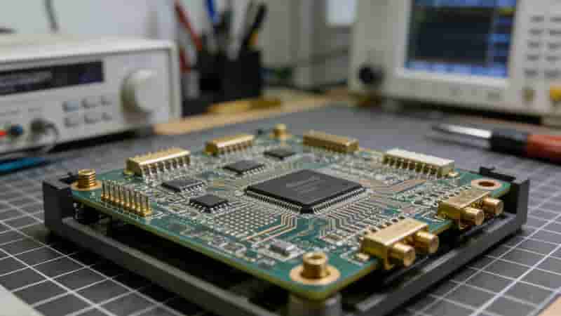
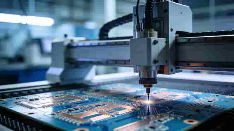
PCBs serve as the foundation for almost all modern electronics. They provide the mechanical structure and electrical connections between components. In order to facilitate these electrical connections, PCBs utilize plated through holes (PTHs) and vias. Both PTHs and vias enable conduction between different layers in multilayer PCB designs. However, confusing these terms can lead to suboptimal PCB design and manufacturing defects.
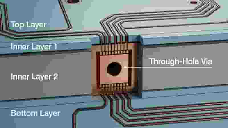
Vias are also vertical interconnects but they are localized connections within or between layers of a PCB. Vias have smaller diameters than PTHs, usually between 0.1mm to 0.5mm. While PTHs function mainly for component connections, vias are primarily used to route signals between traces on different layers. Their purposes focus more on allowing trace routing rather than component placement.
PTH vs Via: Dimensions, Locations and Functions
While PTHs and vias share some high-level similarities as vertical interconnects in multilayer PCBs, they have distinct differences:
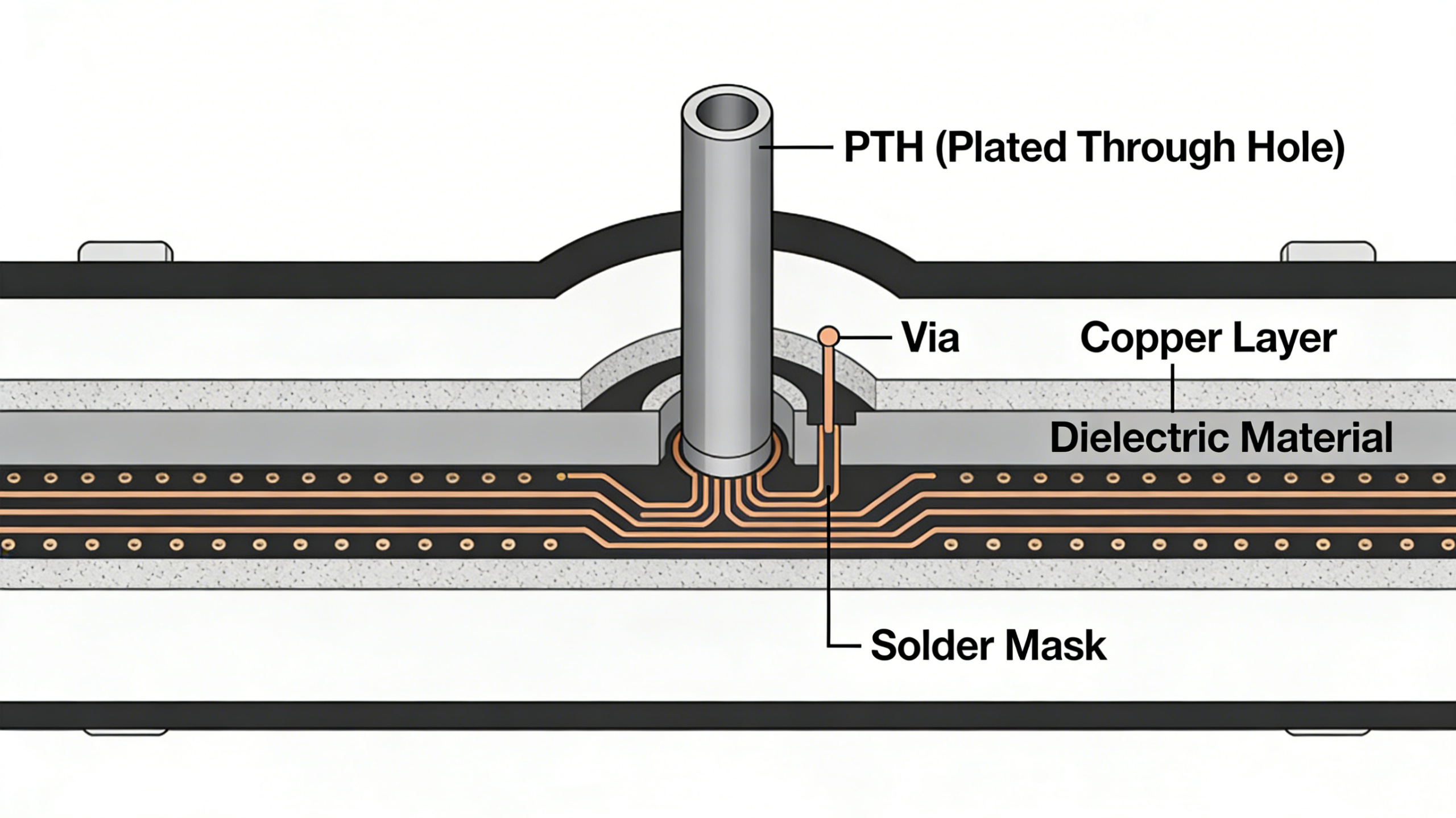
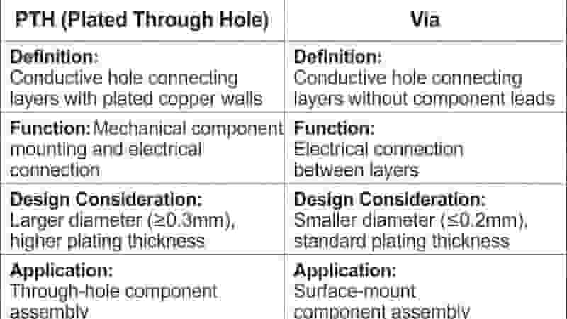
Locations: The most fundamental difference is PTHs span entirely through boards, while vias only connect within or between layers. PTHs make connections through the whole PCB stackup. Vias link traces in planar sections.
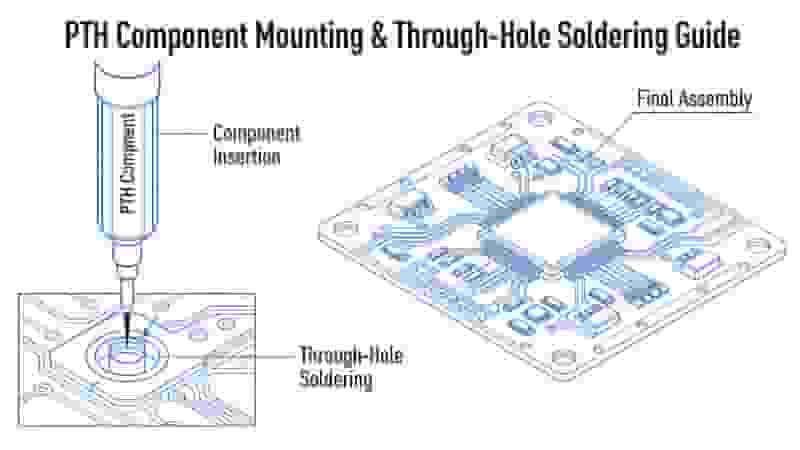
Functions: Due to their placement, PTHs primarily enable mounting and connecting components. The through hole pads provide anchoring points for leads to be soldered. Vias mainly function to reroute signals between layers when optimal trace routing is unavailable on the same plane.
Dimensions: PTHs require larger diameters to accommodate component leads, generally ranging from 0.15mm to 2mm. Vias only need to link thin traces, so appropriately have smaller diameters between 0.1mm to 0.5mm. Narrower dimensions allow higher via densities.
Finishing: For soldering components, PTHs often require solder masking over pads and special hole preparations. Vias do not undergo soldering so lack finishing requirements. No solder masking or hole preparations are involved.
PTH vs. Via – Key Characteristic Comparison
| Feature | Plated Through Hole (PTH) | Via |
|---|---|---|
| Definition | A hole with copper plating | An electrical connection between layers |
| Purpose | Connect layers or mount components | Route signals between layers |
| Size | 0.15mm–2mm diameter | 0.1mm–0.5mm diameter |
| Component Mounting | Supported | Not supported |
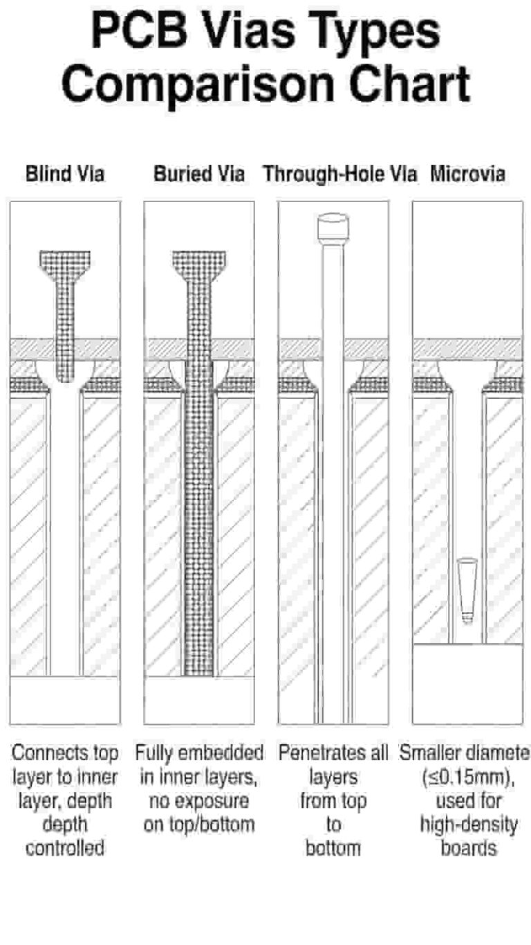
| Types | Single/double/multilayer PTH | Through, blind, buried via |
Real-World Applications: When to Use PTHs and Vias
PTH Applications in PCB design:
- Component lead connections for mechanical anchoring and conductivity
- Multi-layer stacking across full PCB stackups
- Power and ground plane connections
- EMI shielding with grounded PTHs
Via Applications in PCB design:
- Escape routing for congested surface traces
- Layer translation for high-speed signals
- Heat dissipation from SMT pads
- Stitching for improved conductivity
Design Guidelines for Optimal PCB Fabrication
For PTHs: Match hole diameters to component leads; optimize padstack quantity; provide thermal reliefs for high-power connections to protect PCB reliability.
For Vias: Comply with minimum annular ring requirements; control impact on high-speed signal impedance; ensure proper filling to avoid moisture issues in blind and buried vias.
Key Takeaways
In summary, PTHs and vias both enable vertical conductivity in a PCB, but serve different roles. PTHs span the entire board for component mounting, while vias provide compact layer-to-layer signal routing. Correct use improves yield, space efficiency, and signal integrity in PCB design and manufacturing.
We provide professional PCB design support, prototyping, mass production and assembly services for global industrial buyers and engineers.
Get Your PCB Solution Now
Contact us for DFM analysis, free quotation, custom design and reliable manufacturing for your PCB project.
Inquiry & Quote
What is Copper Core PCB? Comprehensive Overview, Advantages & Industry Insights
PCB Drilling Process: Full Technical Guide for Manufacturing & Quality
Why Choose FR-4 as Your PCB Material in 2025? The Definitive Engineer’s Guide
Flexible PCB Cost in 2025: Why It’s Expensive and Proven Ways to Save
How to Choose the Right Quick Turn PCB Assembly Manufacturer