PCBs For New Energy Applications – The Top PCB Partner for Innovations in Energy and Renewable Technologies
Abstract
As global demand for renewable energy grows, PCBs For New Energy Applications have become critical components in solar, wind, energy storage, EV, and fuel cell systems. We specialize in manufacturing high-performance, durable printed circuit boards engineered to withstand high voltages, extreme temperatures, vibration, and harsh operating environments. Our full-service PCB fabrication and assembly solutions support reliable, long-life operation in sustainable energy projects worldwide.
Types of PCBs For New Energy Applications
PCBs For New Energy Applications require specialized designs to meet high-power, thermal, and reliability demands. Below are the most widely used types:
- High Voltage PCBs: Engineered for voltages over 1,000V with strict isolation and layout design.
- Thick Copper PCBs: Support high current loads up to 400A+ with low resistance and heat generation.
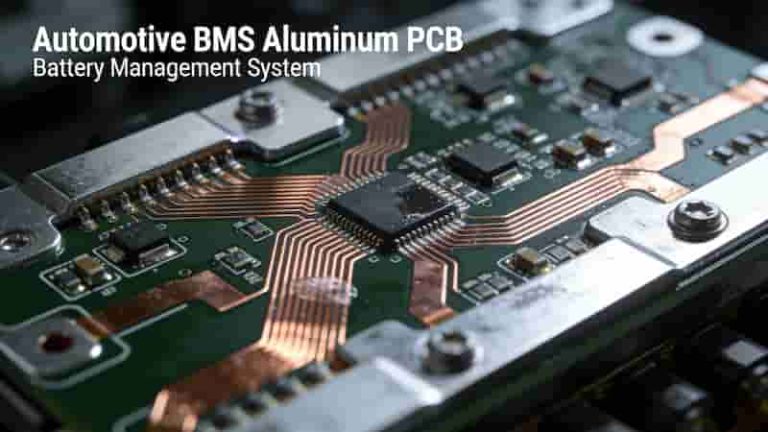
- Aluminum & Metal Core PCBs: Excellent thermal conductivity for high-power heat dissipation.
- High Frequency PCBs: Ensure signal integrity in telemetry and communication modules.
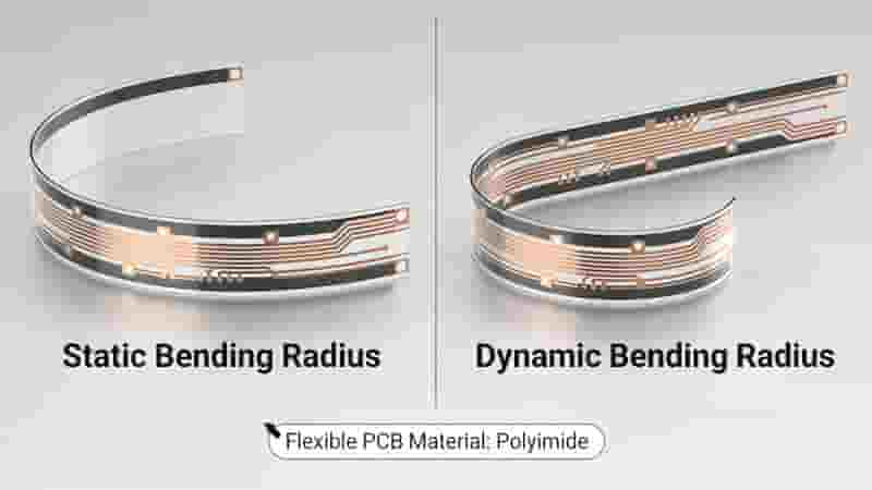
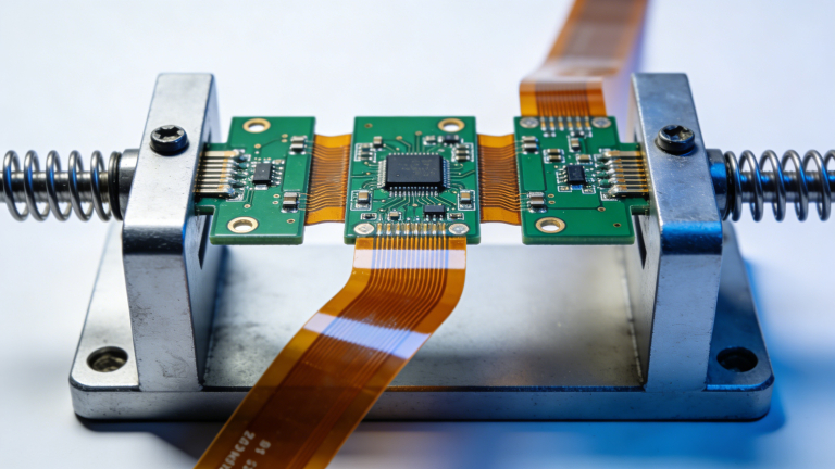
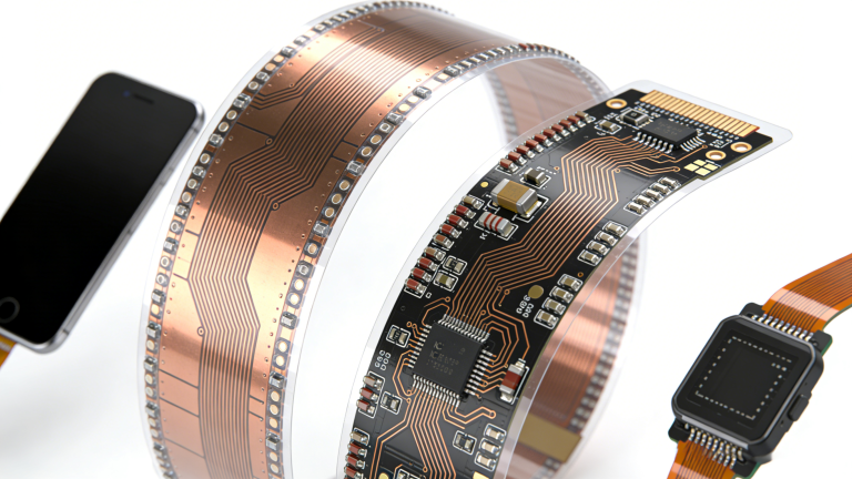
- Flex & Rigid-Flex PCBs: Resist vibration, shock, and bending in dynamic installations.

Key Specifications for New Energy PCBs
PCBs For New Energy Applications must meet strict performance standards for industrial and renewable energy systems:
- High voltage isolation: 1000V+ AC/DC insulation resistance
- High current capacity: 100A-400A+ thick copper traces
- Wide temperature range: -40°C to +150°C or higher
- Controlled impedance and stable signal integrity
- Superior thermal management and heat dissipation
- Compliance with IPC, RoHS, REACH, and ISO standards

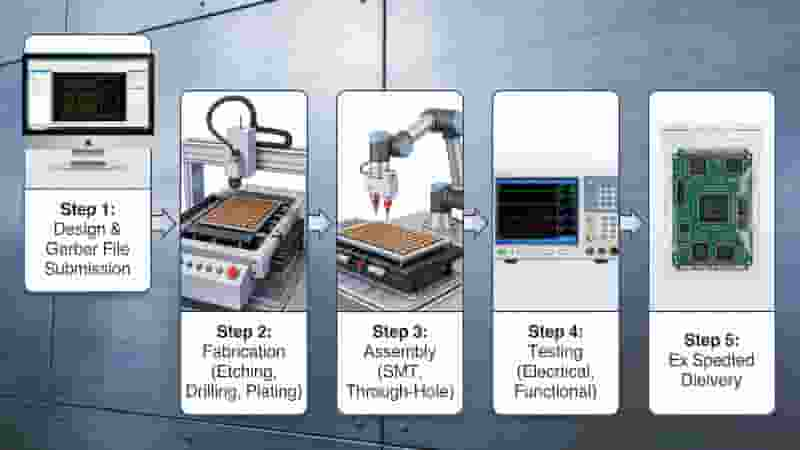
Our PCB Manufacturing & Assembly Services
We provide end-to-end solutions for PCBs For New Energy Applications from prototype to mass production:
Fabrication Capabilities
- Multilayer boards up to 32+ layers for power electronics
- Blind/buried vias for space-efficient design
- Flex, rigid-flex, and metal core constructions
- ENIG, immersion tin, and lead-free surface finishes
- Fast prototype delivery in 24 hours
Assembly Capabilities
- High-precision SMT assembly for 01005 components
- Through-hole, selective, and busbar soldering
- 3D SPI, AOI, X-ray inspection and full testing
- Burn-in, validation, and lifecycle reliability testing
Main Applications in New Energy Systems
PCBs For New Energy Applications are widely used across core renewable energy sectors:
- Solar Power Systems: Solar inverters, MPPT controllers, grid-tie systems
- Wind Turbines: Pitch control, converters, monitoring and grid integration
- Energy Storage Systems: BMS boards, battery packs, power distribution
- EV & EV Charging: Onboard chargers, DC-DC converters, charging stations
- Hydropower & Fuel Cells: Control units, power conversion, safety systems

Environmental & Compliance Standards
Our PCBs For New Energy Applications follow green manufacturing and global compliance requirements:
- RoHS, REACH, and conflict mineral compliance
- Lead-free and halogen-free materials and processes
- ISO 9001, ISO 14001, IATF 16949 certified systems
- Eco-friendly production, waste reduction, and recycling
Why Choose Us for PCBs For New Energy Applications
We are a trusted global partner for renewable energy PCB solutions:
- 15+ years of experience in new energy and power electronics
- Full in-house fabrication, assembly, and testing capabilities
- Custom design support and DFM optimization
- Competitive pricing and fast, reliable lead times
- Dedicated engineering and customer support team
Summary
PCBs For New Energy Applications are foundational to modern renewable energy systems. We deliver high-reliability, custom-designed printed circuit boards that meet the strict demands of solar, wind, energy storage, EV, and fuel cell applications. With advanced manufacturing, strict quality control, and full compliance, we support sustainable energy innovation worldwide.
Ready to Start Your New Energy PCB Project?
Get a free, no-obligation quote for your PCBs For New Energy Applications today.
Contact us for:
- Custom PCB design and DFM review
- Prototype and mass production solutions
- Technical support and material selection
- Fast quotation and responsive service
Email us now to receive your optimized PCB solution for new energy applications.
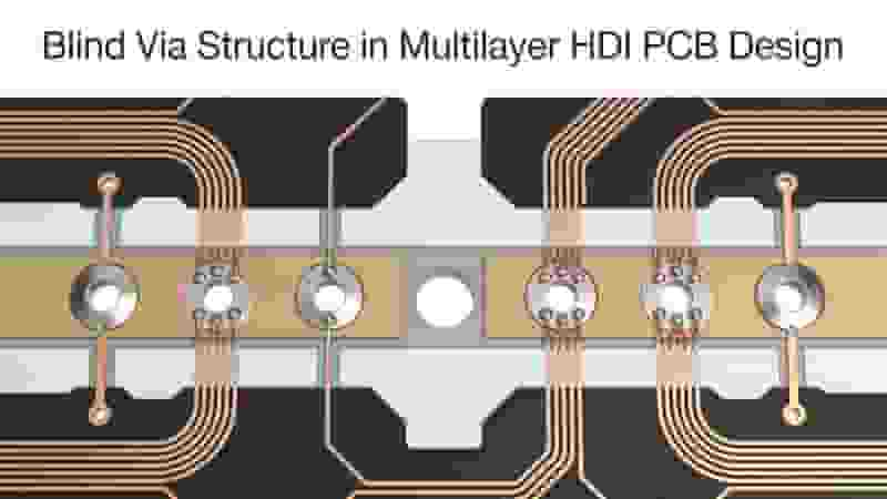
Blind Vias & Buried Vias in PCBs – The Complete Engineering Guide
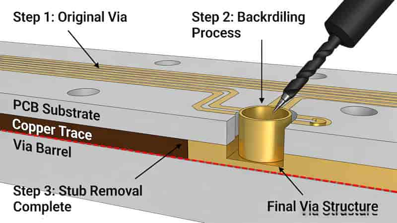
Backdrilling of Vias: The Definitive Guide for High-Speed PCB Signal Integrity
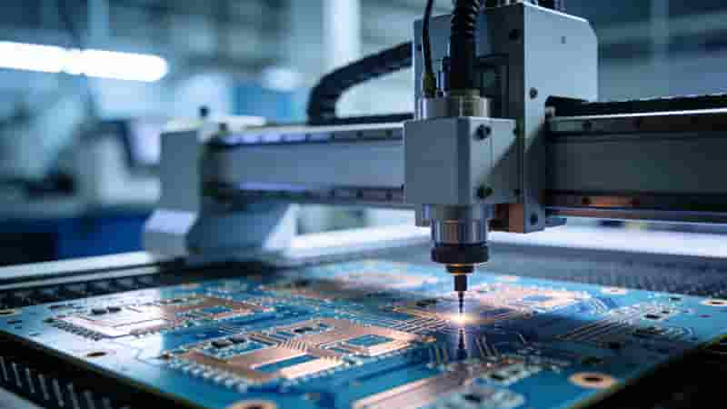
PCB Drilling Process: Full Technical Guide for Manufacturing & Quality
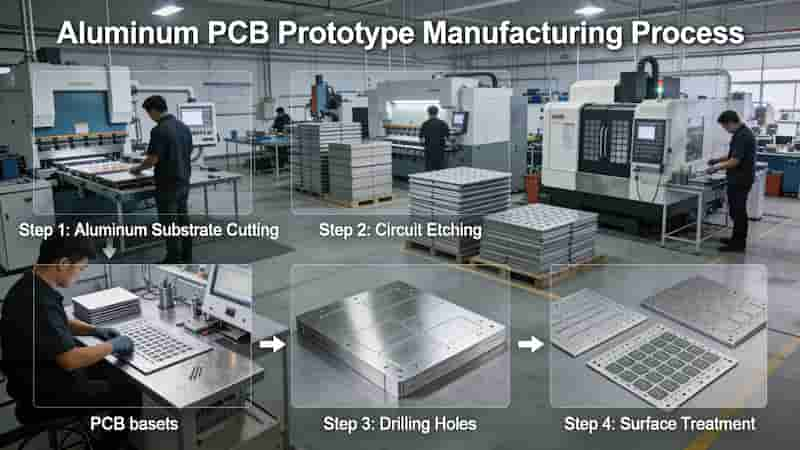
Aluminum PCB Prototype: The Ultimate Guide for Engineers and Designers
Expedited PCB Services – Fast Turnaround for Urgent Prototypes & Production