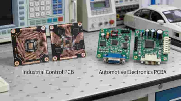
We provide reliable through-hole PCBAs assembly service for industrial, power, medical, aerospace and automotive applications. Our IPC-standard THT assembly supports prototypes to mass production with wave soldering, selective soldering and full inspection.
Through-hole PCB Assembly Service Overview
Our through-hole PCB assembly fulfills leaded assembly demands across industries. We deliver single-sided, double-sided and high-density multilayer through-hole PCB assembly to support low to mid-volume production.
Two dominant assembly methods exist for PCB components: Through-hole Assembly and Surface Mount Technology. We provide one-stop through-hole PCB assembly from prototyping to mass production with full turnkey support.
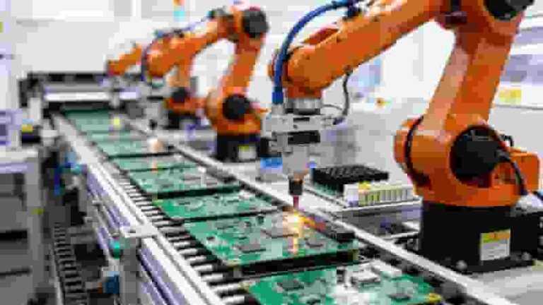
We combine manual and automated assembly techniques to ensure high quality and cost efficiency. Complex assemblies use manual insertion, while automated lines suit stable volume runs.
Introduction to Through-hole Technology (THT)
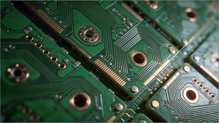
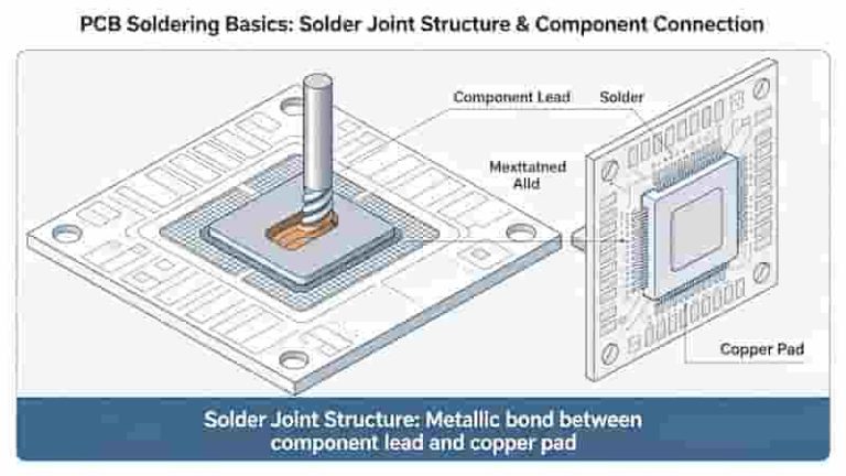
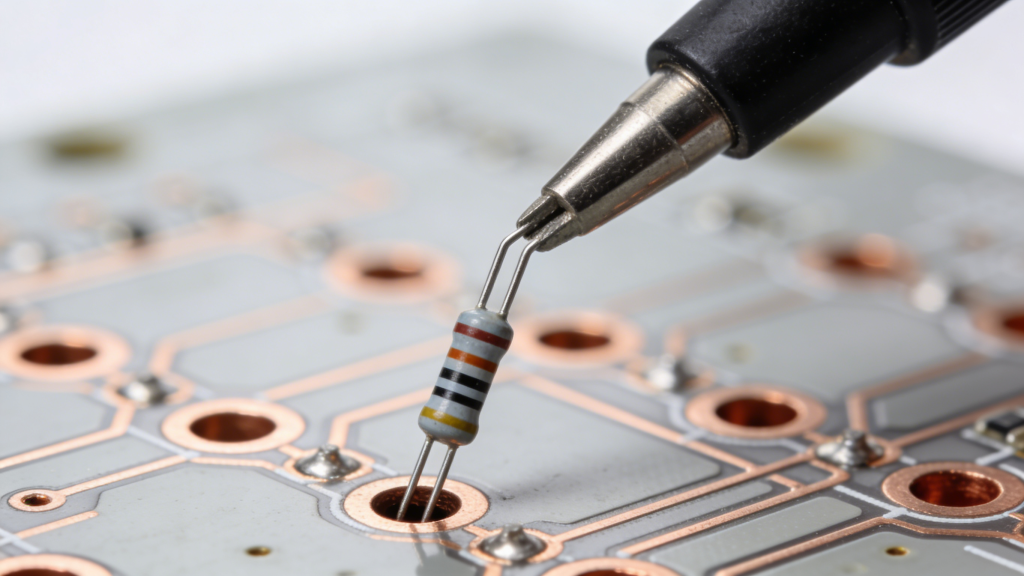
Through-hole PCB assembly is a process where component leads are inserted into drilled holes on a bare PCB and soldered to pads on the opposite side. It can be completed via manual assembly or automated insertion machines.
THT remains a critical mounting technology widely used in high-reliability electronics. Key features include:
- Manual and automated component insertion
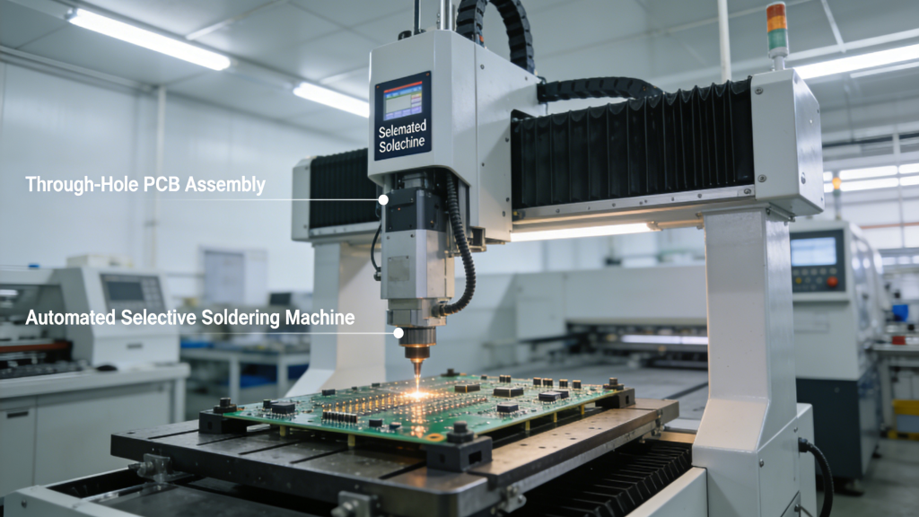
- Wave soldering or selective soldering applied
- Radial or axial lead components supported
- Ideal for military, aerospace and high-Tg applications
- Components mounted vertically or horizontally
Why Choose Through-hole PCB Assembly
Through-hole PCB assembly offers stronger mechanical strength than most surface mount connections. THT leads run through the entire board, creating bonds that withstand extreme vibration, shock and high temperature.
This makes through-hole PCB assembly ideal for military, automotive and aerospace products exposed to harsh environments. It also supports easy prototyping, manual adjustment and component replacement.
Core Benefits:
- High mechanical strength and compression resistance
- Excellent heat tolerance for high-power applications
- Superior long-term reliability and durability
- Easy prototyping, rework and component replacement
- Strong solder bonds resistant to environmental stress
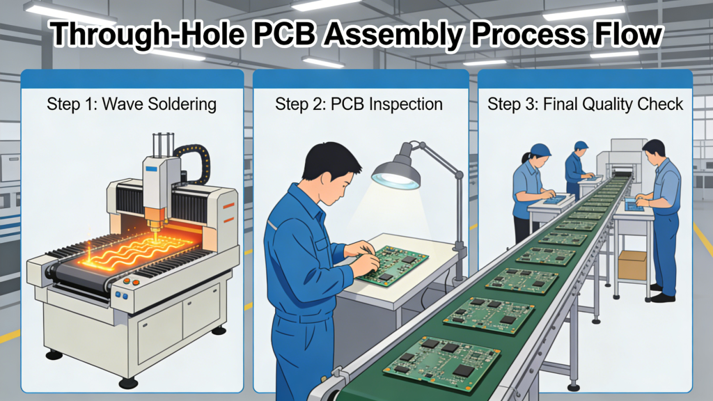
Through-hole PCB Assembly Process
Our through-hole PCB assembly follows strict IPC standards to ensure consistency and quality:
- PCB fabrication (single or panel)
- Component insertion (manual or automated)
- Soldering (wave, selective or hand soldering)
- Cleaning (aqueous or ultrasonic)
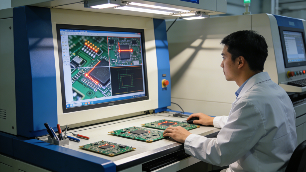
- Inspection (AOI, X-ray, visual)
- Electrical testing (ICT, FCT)
- Panel breakaway and final packaging
THT vs SMT PCB Assembly Comparison
| Item | Through-hole PCB Assembly | SMT Assembly |
|---|---|---|
| Mechanical Strength | High, through-board connection | Medium, surface-mounted |
| Component Size | Larger, high-power parts | Miniature, high-density |
| Best For | High-reliability, harsh environments | Consumer electronics, compact design |
| Rework | Easy to replace components | Special tools required |
Through-hole PCB Assembly Service Capabilities
Our full through-hole PCB assembly capabilities cover simple to complex projects:
- Manual & automated axial/radial insertion
- Leaded & RoHS-compliant lead-free soldering
- Wave soldering & computer-controlled selective soldering
- Conformal coating & in-circuit device programming
- Built to IPC-A-610 and J-STD-001 standards
Board & Component Support:
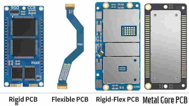
- FR-4, aluminum, copper-core, rigid-flex boards
- Connectors, relays, high-power components
- Size range: 0.2″×0.2″ to 15″×20″
- Prototype to mid-volume production
Testing & Inspection for Through-hole PCB Assembly
We ensure every through-hole PCB assembly meets strict quality standards with full testing:
- Automated Optical Inspection (AOI)
- Automated X-Ray Inspection (AXI)
- In-Circuit Test (ICT)
- Functional Circuit Test (FCT)
- Burn-in test & assisted visual inspection
- First Article Inspection (FAI) available
Summary
Through-hole PCB assembly remains essential for high-reliability electronics requiring strong mechanical bonds, heat resistance and durability. Our professional through-hole PCB assembly service delivers IPC-certified quality, flexible production and full testing for industrial, medical, aerospace and automotive applications.
We provide one-stop turnkey solutions from PCB fabrication and component sourcing to assembly, testing and delivery, ensuring fast turnaround and stable quality for global buyers.
Request Your Through-hole PCB Assembly Quote
Send us your BOM, Gerber files and assembly requirements. We provide DFM review, competitive pricing and fast lead times for your through-hole PCB assembly project.
Contact Us for a Free Quote
How to Effectively Clean PCB Assembled Boards for Optimal Performance
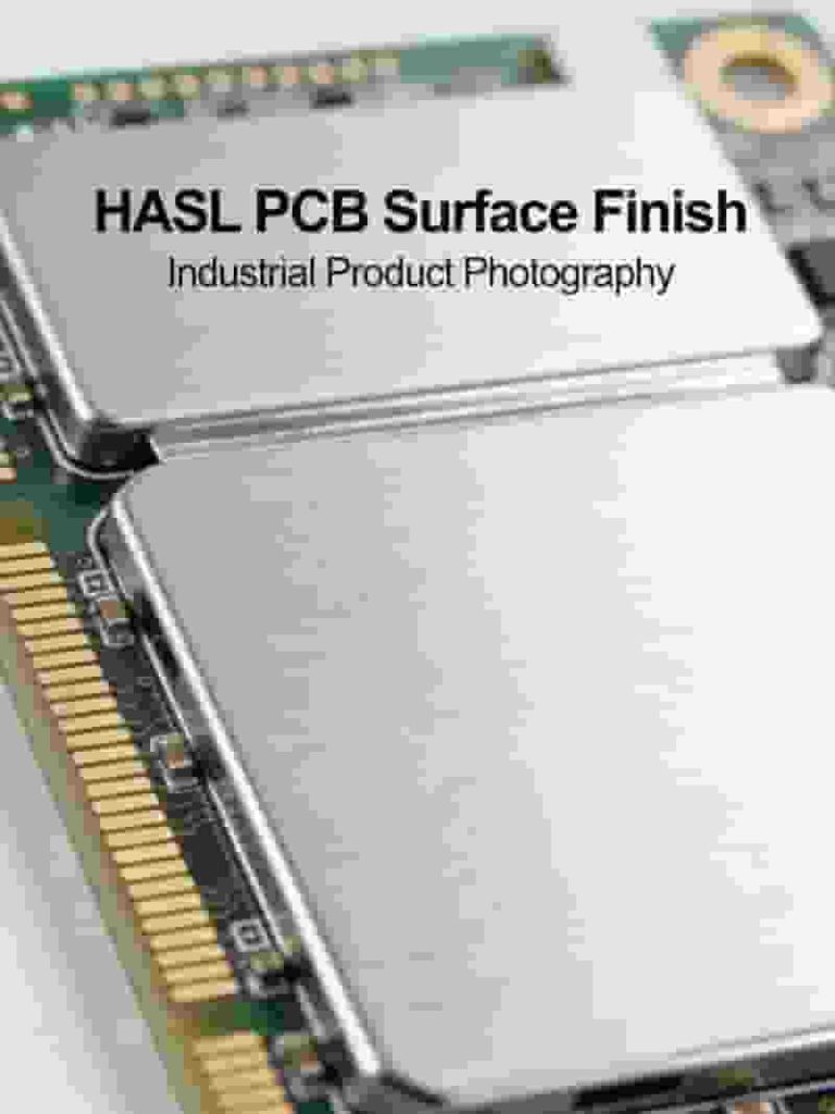
HASL: Hot Air Solder Leveling for PCB Surface Finish
Quick Turn PCB Assembly Services for Fast Prototypes and Production
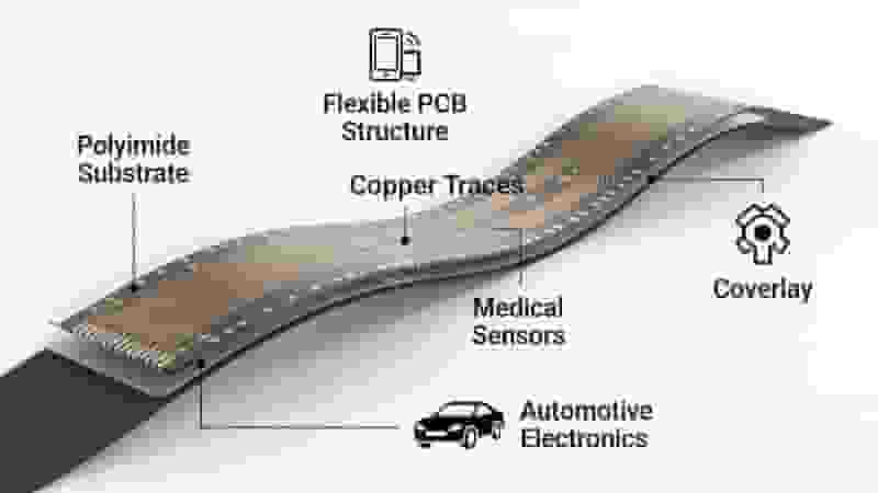
Flexible PCB Manufacturing Process Steps: Complete Technical Guide
PCB Manufacturer in South Africa | Local PCB Manufacturing & Export