Double sided PCB assembly supports high‑density circuit design by mounting components on both top and bottom sides of the board. This professional guide explains core definitions, full manufacturing processes, soldering technologies, pros and cons, design best practices, quality control, and application scenarios to help industrial buyers, engineers and procurement teams make informed decisions.
What Is Double Sided PCB Assembly
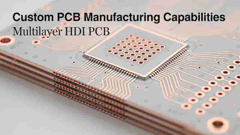
Double sided PCB assembly refers to the process of mounting electronic components on both the top and bottom surfaces of a printed circuit board. Unlike single‑sided boards, it uses plated through‑holes (PTH) or vias to connect circuits between two layers, greatly improving wiring density and space utilization.
This technology is widely used in consumer electronics, industrial control, automotive electronics, medical devices and communications equipment, providing a cost‑effective solution for medium‑complexity circuit designs.
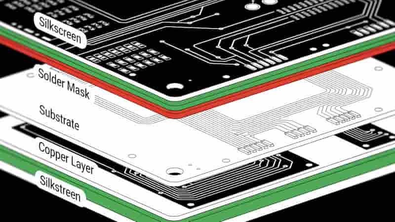
Core Structure & Components
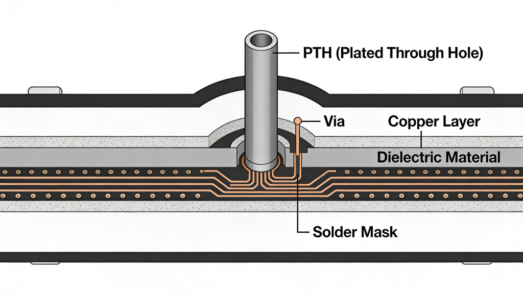
A standard double sided PCB consists of four key structural layers, each with a clear functional purpose:
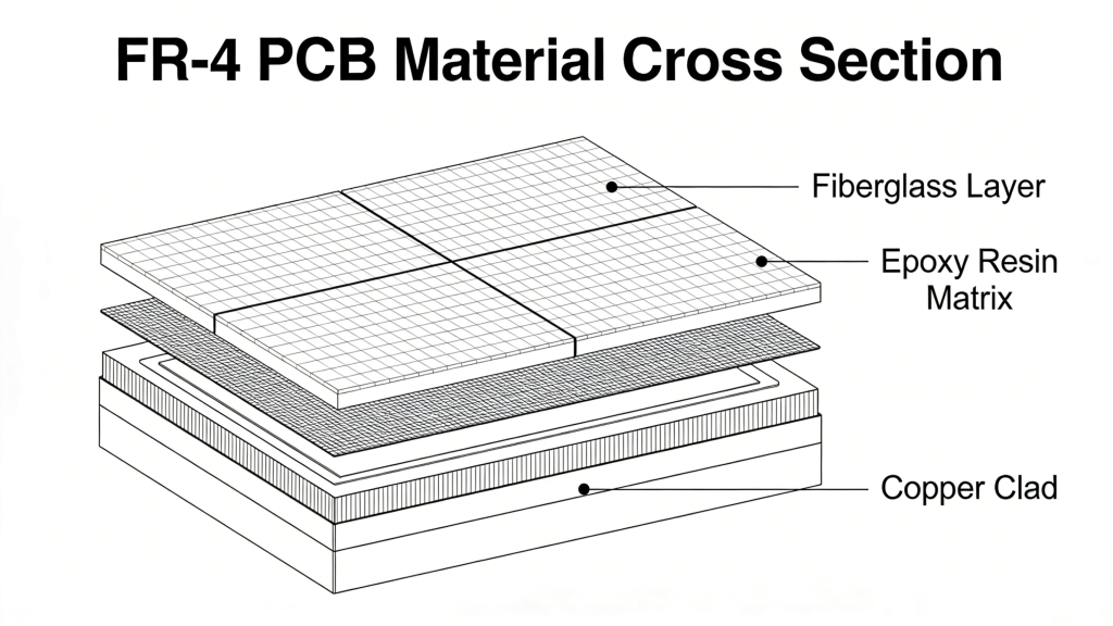
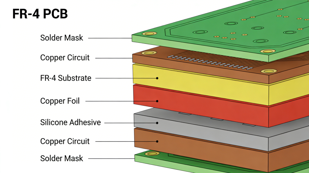
- Substrate: Usually FR‑4 material, providing mechanical support and insulation
- Copper Layers: Double‑sided copper foil etched into circuit traces and pads
- Solder Mask: Protective layer to prevent short circuits and oxidation
- Silkscreen: Markings for component orientation, polarity and assembly notes
Plated vias are the key to connecting two layers, enabling reliable electrical connection in double sided PCB assembly.
Double Sided vs Single Sided PCB
| Item | Single Sided PCB | Double Sided PCB |
|---|---|---|
| Component Placement | One side only | Both top and bottom sides |
| Circuit Complexity | Low, simple circuits | Medium, high‑density routing |
| Size | Larger for same function | Compact, space‑saving |
| Cost | Lower | Moderate |
| Typical Use | Toys, simple controls | Industrial, automotive, consumer electronics |
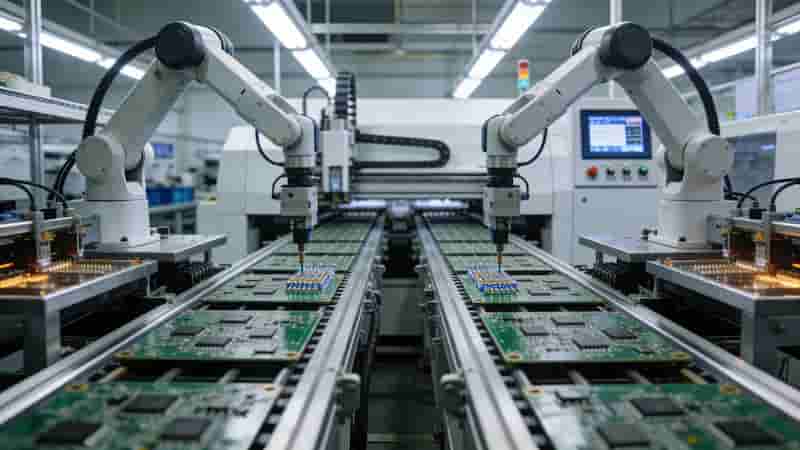
Full Double Sided PCB Assembly Process
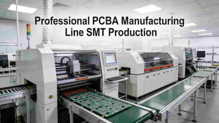
The complete double sided PCB assembly process includes SMT and THT assembly, with strict process control to ensure stability and consistency.
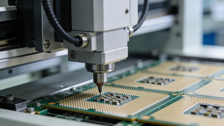
1. SMT Assembly (Double‑Sided)
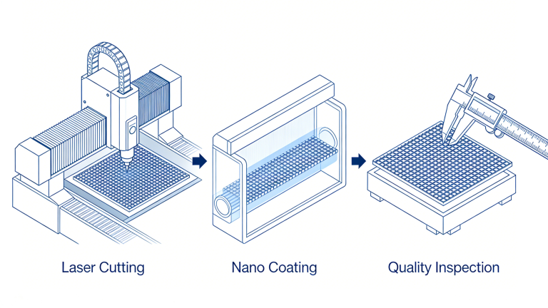
- Solder paste printing through laser stencil
- Pick‑and‑place SMD components on first side
- Reflow soldering to fix components
- Flip board, apply adhesive for bottom components
- Repeat printing, placement and reflow for second side
2. Through‑Hole (THT) Assembly
- Insert through‑hole components into drilled holes
- Wave soldering or selective soldering for reliable connection
- Cut excess leads and clean the board
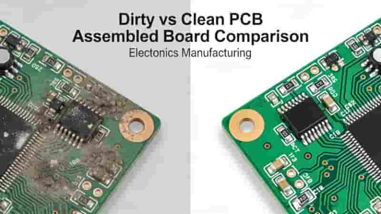
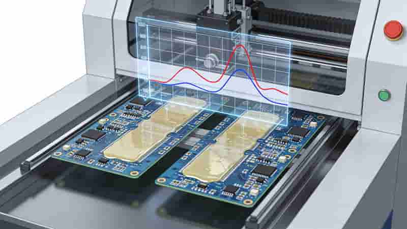
3. Cleaning & Inspection
Remove flux residues; use AOI, X‑ray and electrical testing to verify assembly quality of double sided PCB assembly.
Soldering Techniques for Double Sided PCB
Different soldering methods apply to different production scenarios in double sided PCB assembly:
- Reflow Soldering: Mainstream for SMT components, stable and high‑efficiency
- Wave Soldering: Suitable for through‑hole parts on the bottom side
- Selective Soldering: Protects sensitive components during mixed assembly
- Hand Soldering: For prototypes and small‑batch repairs
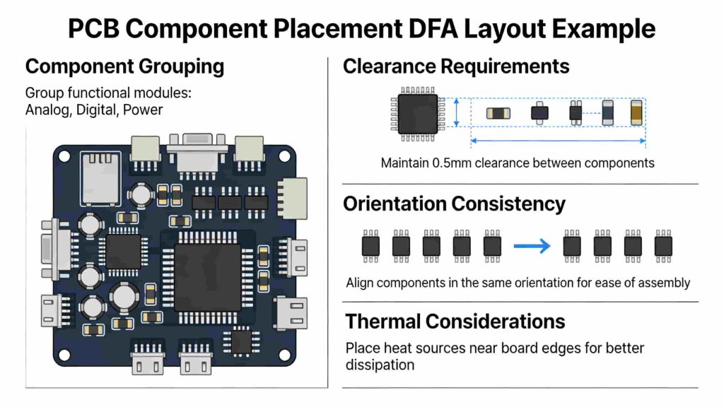
Design & DFM Guidelines
Reasonable design directly improves the yield and reliability of double sided PCB assembly:
- Optimize component layout to reduce cross interference
- Reasonably arrange vias and avoid affecting component placement
- Set sufficient edge clearance for assembly equipment
- Add thermal vias for high‑power components
- Comply with IPC standards for DFM review
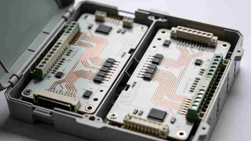
Industry Applications
Double sided PCB assembly serves most medium‑complexity electronic products:
- Consumer electronics: smartphones, tablets, smart home devices
- Industrial control: PLC, drivers, sensors, automation equipment
- Automotive: on‑board controllers, dashboards, lighting systems
- Medical: portable devices, monitoring instruments
- Communications: network modules, IoT terminal devices
Quality Control & Testing
We implement full‑process quality control for double sided PCB assembly:
- AOI automatic optical inspection for assembly defects
- X‑ray inspection for BGA, QFN and hidden solder joints
- ICT in‑circuit test for electrical connectivity
- Functional test to simulate real working conditions
- Full IPC‑A‑610 standard compliance
Conclusion
Double sided PCB assembly provides an ideal balance of density, performance, size and cost for modern electronics. It supports both SMT and THT processes, adapts to medium‑complexity design requirements, and is widely used in many industries.
With professional manufacturing processes, strict quality control and optimized DFM design, we provide stable and reliable double sided PCB assembly services for global industrial buyers, engineers and procurement teams.
Need Professional Double Sided PCB Assembly?
We offer turnkey double sided PCB assembly, prototype to mass production, DFM review, full testing and global delivery. Get free quote and project support now.
Request Free Quote
PCB DFM and DFA: Best Practices for Optimal Design
Why Choose FR-4 PCBs in 2025? Benefits, Applications & Custom Solutions for 5G, IoT & EVs
The Essentials of Microvias – Enabling Miniaturization in PCBs
What is FR-4 Material in PCB Fabrication? Complete Engineering Guide
What is the Difference Between PTH and Via in PCBs?