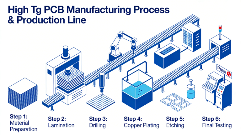
Step stencils optimize solder paste deposition for mixed-component PCBs, improving yield, reliability, and first-pass success in SMT assembly for electronics, automotive, and medical devices.
Imagine a production line where tiny 01005 components sit alongside large edge connectors on a single printed circuit board. The challenge? Applying just the right amount of solder paste to each component without defects. This is where step stencil technology shines, offering a tailored solution for today’s complex PCB assembly processes.
What Are Step Stencils?
Step stencils are advanced SMT tools used to apply solder paste onto PCBs. Unlike standard stencils with uniform thickness, step stencils feature varying foil thicknesses to match the requirements of different components.
Per IPC 7525B Stencil Design Guidelines (2011), a step stencil is defined as “a stencil with more than one foil thickness level.” This design solves critical challenges in modern PCB manufacturing.
Step-Down Stencils: Thinner regions for miniature components (01005, 03015, fine-pitch ICs) ensure clean paste release and reduce defects in compact electronics.
Step-Up Stencils: Thicker regions for large components (BGAs, D-PAKs, power connectors) deposit sufficient paste for robust, high-reliability joints.
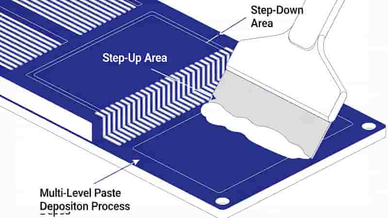
Multi-Level Step Stencil for PCB Assembly
How Step Stencils Are Made
Three professional manufacturing methods deliver step stencil performance for industrial PCB production:
1. Photo-Chemical Etching
Cost-effective for high-volume runs; however, precision can vary, often over-etching step depths.
2. Laser Welded Technology
Extremely accurate step depths, ideal for high-complexity PCB designs; slightly higher cost but superior consistency.
3. Micro-Machining Technology
Highest accuracy and smooth surface finish, greatly improving paste release; best for medical and automotive-grade PCBs.
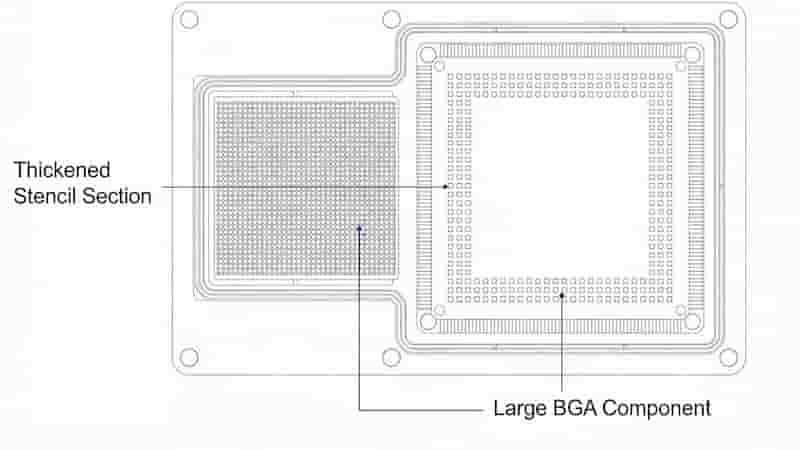
Step Up Stencil Structure
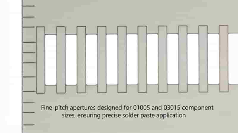
Step Down Stencil for Fine-Pitch Parts
Experimental Insights & Performance
Independent printing tests compare step stencil performance using 4-mil base foils with 2.0, 2.5, and 3.0 mil step-downs, tested with 03015, 01005, 0.3mm–0.5mm BGAs, and QFNs.
Key results confirm that step stencils with FPN (Fluoro-Polymer Nano) coating provide higher and more consistent solder paste volume, lower defect rates, and better release properties.
Laser-welded and micro-machined models show near-perfect step depth accuracy, making them preferred for mission-critical PCB assembly.
Why Step Stencils Matter
Step stencils solve the core challenge of mixed-technology PCBs where small and large components coexist. They deliver:
- Stable, reliable solder joints for automotive, medical, and industrial electronics
- Reduced assembly defects and lower rework costs in PCB manufacturing
- Higher first-pass yield and faster production throughput
- One-stencil solution for diverse component sizes
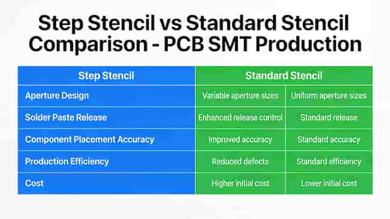
Standard vs Step Stencils Comparison
| Feature | Standard Stencil | Step Stencil |
|---|---|---|
| Thickness | Uniform | Multi‑level |
| Best For | Simple PCBs | Mixed‑component PCB Assembly |
| Defect Rate | Higher | Lower |
| Industry Fit | Basic electronics | Auto, Medical, High‑Tech PCB |
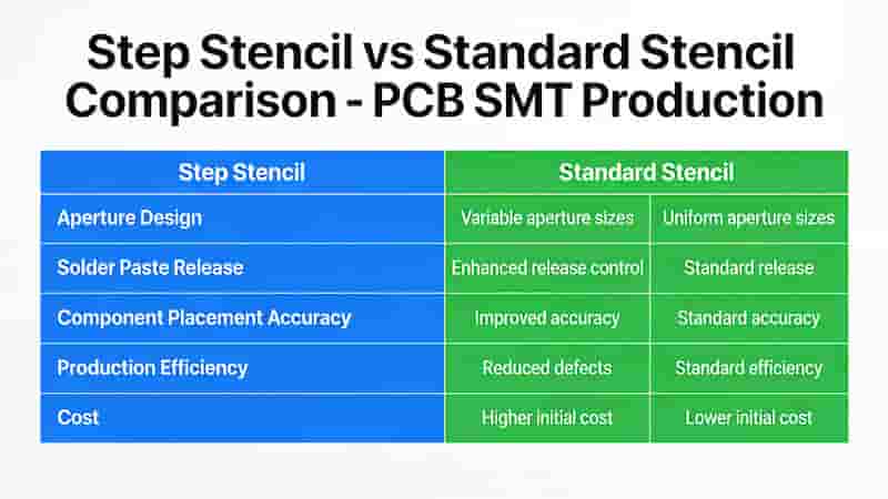
Step Stencil vs Standard Stencil
Conclusion
Step stencil technology is essential for modern PCB assembly, supporting miniaturization, high reliability, and mixed-component designs used worldwide. From consumer electronics to electric vehicles and medical devices, step stencils ensure consistent, high-quality solder paste deposition that directly improves product performance and longevity.
Get Precision Step Stencils for Your PCB Projects
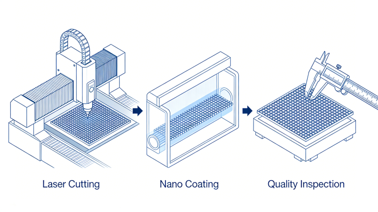
We provide custom step stencils, laser-cut SMT stencils, and nano-coated stencils optimized for your PCB assembly line.
Request a Quote
|
Contact Us for Custom Solutions