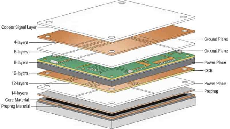
We offer professional multilayer PCB manufacturing services in China supporting 4 to 30 layer rigid, flex, and rigid-flex PCBs. Our high-reliability boards serve industrial, telecom, medical, aerospace, and automotive applications with ISO 9001, IATF 16949, IPC-A-610 Class 3, UL, and RoHS compliance.
Multilayer PCB Manufacturing Capabilities
We provide comprehensive multilayer PCB manufacturing with precise specifications to meet complex engineering requirements:
| Feature | Specifications |
|---|---|
| Layer Count | Rigid: 4 to 30 layers; Flex: up to 10 layers; Rigid-Flex: up to 8 layers |
| Base Materials | FR4, High-Tg FR4, High-Frequency, Polyimide |
| Board Thickness | Rigid: 0.4 to 6.0 mm; Flex: 0.1 to 0.8 mm; Rigid-Flex: 0.25 to 2.0 mm |
| Copper Weight | 0.5 to 6 oz (inner & outer layers customizable) |
| Surface Finishes | Lead-free HASL, ENIG, Immersion Silver, Immersion Tin, Hard Gold |
| Testing | AOI, Flying-Probe, Impedance Control, Thermal Shock |
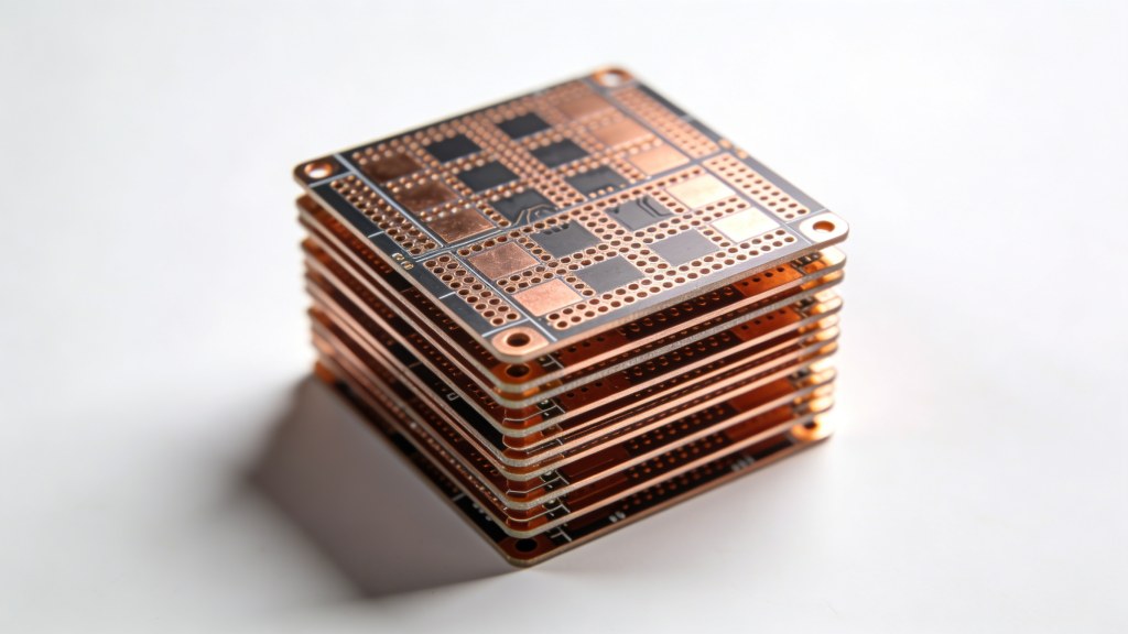
Types of Multilayer PCB We Manufacture
We specialize in diverse multilayer PCB types for various applications:
Rigid Multilayer PCB
Stable structure for industrial, telecom, and computing applications with consistent electrical performance.
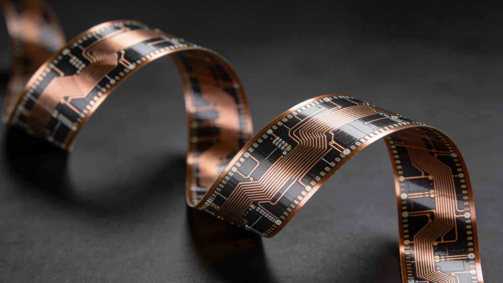
Flexible Multilayer PCB
Polyimide-based boards for bending, folding, and space-constrained wearable & compact electronics.
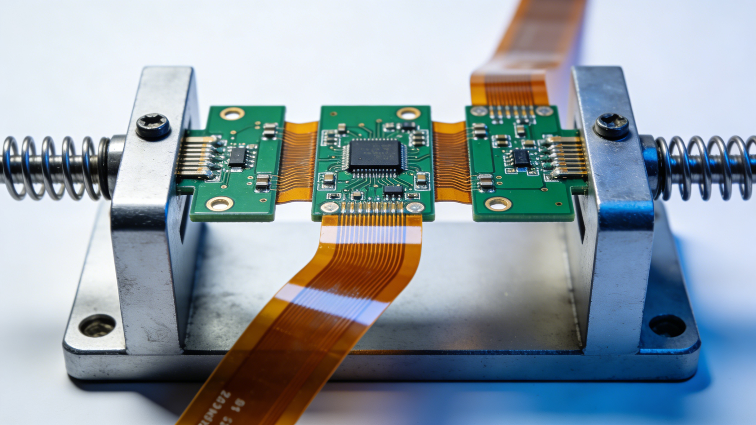
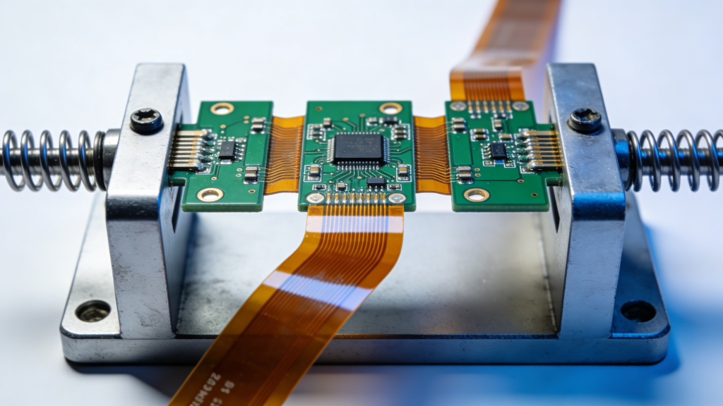
Rigid-Flex Multilayer PCB
Combines rigid and flexible sections for aerospace, medical, and high-vibration environments.
HDI & High-Speed Multilayer PCB
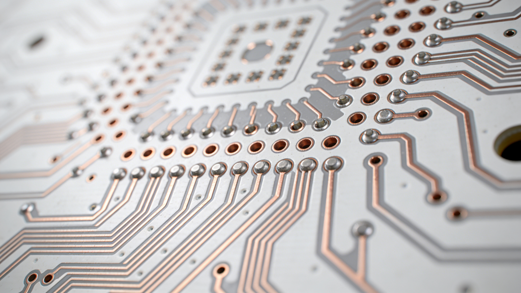
Fine lines, microvias, and controlled impedance for high-frequency telecom and data systems.
Metal-Based Multilayer PCB
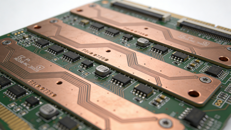
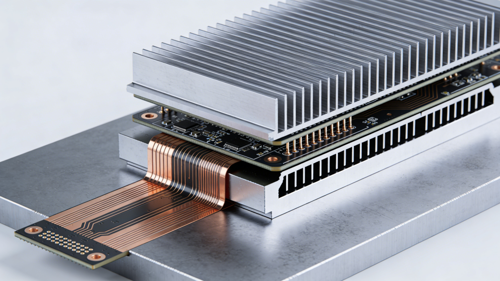
Superior heat dissipation for power electronics and LED systems with high thermal requirements.
Industries Served by Our Multilayer PCB Manufacturing
Our multilayer PCB manufacturing services in China support critical industries worldwide:
- Industrial Control: Stable performance in harsh operating environments
- Telecommunication: High-density routing and signal integrity for networking equipment
- Medical Devices: Precise, reliable PCBs for diagnostic and therapeutic equipment
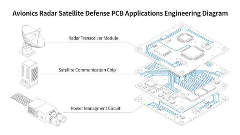
- Aerospace & Defense: Robust construction for mission-critical systems
- Automotive Electronics: IATF 16949 certified boards for vehicle systems
- Wearable Electronics: Compact, flexible designs for portable devices
Why Choose Our Multilayer PCB Manufacturing Services
We deliver reliable multilayer PCB solutions with distinct advantages:
- 15+ Years Expertise: Extensive experience in complex, reliability-critical PCB manufacturing
- Professional DFM Support: Free Gerber review and stack-up optimization
- Full-Service Capability: One-stop rigid, flex, and rigid-flex PCB production
- Stringent Quality Control: Multiple testing procedures ensure consistent quality
- Customization: Tailored materials, layer counts, and specifications
- Competitive Pricing: Cost-effective China manufacturing without quality compromise
Multilayer PCB Manufacturing Process
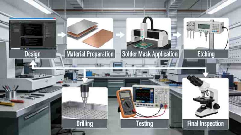
Our precise manufacturing process ensures high-quality multilayer PCB production:
- Engineering Review: Design verification and manufacturability assessment
- Material Preparation: High-quality laminates and conductive materials
- Inner Layer Fabrication: Precise imaging and etching of internal circuits
- Lamination & Drilling: Layer bonding and via formation
- Plating & Outer Layer Processing: Conductive connection and outer circuit formation
- Solder Mask & Surface Finish: Circuit protection and assembly preparation
- Testing & Inspection: Comprehensive quality verification before shipment
Quality Control for Multilayer PCB
Quality is integrated into every stage of our multilayer PCB manufacturing:
- Pre-production engineering review to eliminate design risks
- Real-time process monitoring for consistent production
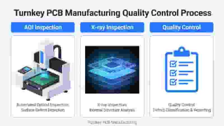
- Automated Optical Inspection (AOI) for circuit accuracy
- Electrical and flying-probe testing for connectivity verification
- Impedance control and reliability testing for performance validation
- Final inspection before shipment to ensure compliance
Multilayer PCB vs. Single/Double-Sided PCB
| Aspect | Single/Double-Sided PCB | Multilayer PCB |
|---|---|---|
| Circuit Complexity | Simple, low-density designs | Complex, high-density applications |
| Space Efficiency | Larger footprint required | Compact, space-saving design |
| Electrical Performance | Basic signal management | Superior signal integrity & grounding |
| Typical Applications | Simple consumer electronics | Industrial, medical, aerospace systems |
Summary
As a leading provider of multilayer PCB manufacturing services in China, we deliver high-reliability rigid, flex, and rigid-flex PCBs for demanding industrial, medical, aerospace, and telecom applications. With advanced manufacturing capabilities, stringent quality control, professional engineering support, and competitive pricing, we are your trusted partner for all multilayer PCB requirements.
Request a Multilayer PCB Quote
Get a customized quote for your multilayer PCB project. Send your Gerber files and specifications for DFM review and competitive pricing.
Get Multilayer PCB Quote
Upload Gerber Files
All engineering files are kept strictly confidential. Fast lead times available for prototype and production orders.
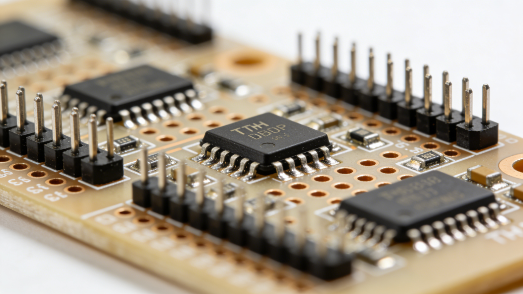
Demystifying THT PCB Assembly: A Comprehensive Professional Guide
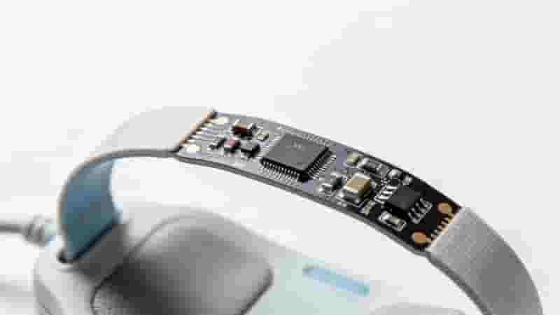
Flexible PCB Stiffeners: Materials, Benefits & Industrial Uses
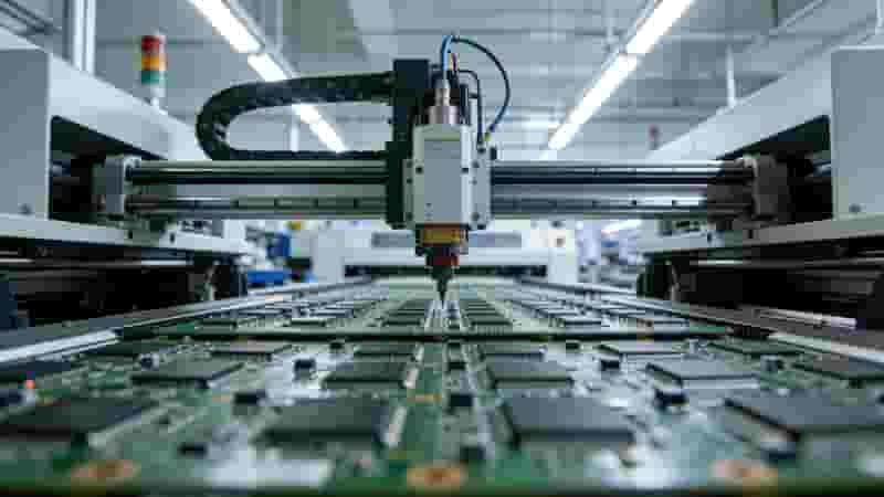
Low-Volume & Small Batch PCB Assembly Service
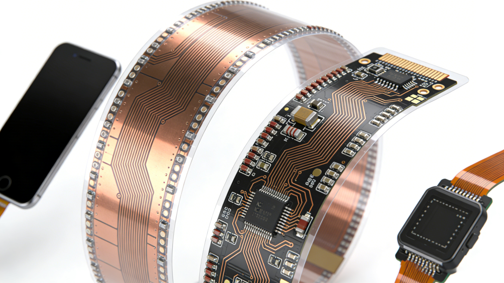
Top 8 Applications of Flexible PCBs for Industrial & Electronics Manufacturing
What is a Surface Mount Device or SMD Component Package?