Rigid-flex PCB stackup combines rigid and flexible layers for compact, reliable designs. Explore its types, design tips, and applications in this professional guide.
Introduction to Rigid-Flex PCB
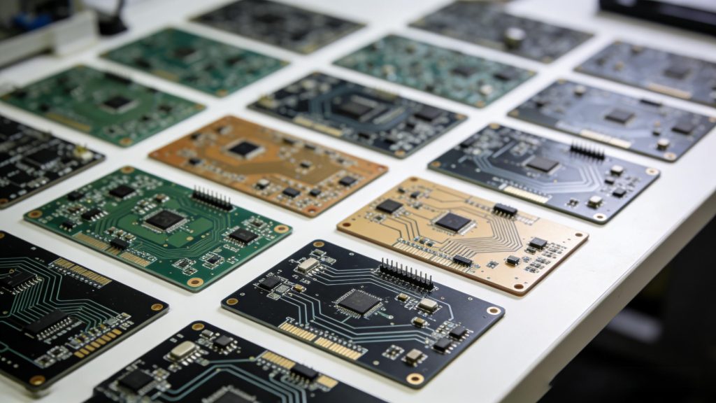
Rigid-flex PCBs combine the strengths of rigid and flexible circuits, creating a hybrid solution for complex, high-density electronic designs. Integrated by plated through holes (PTH), these boards support 3D assembly and are widely used in aerospace, medical, automotive, and consumer electronics. This guide covers core knowledge about rigid flex pcb stackup design and manufacturing.
What is Rigid-Flex PCB Stackup?
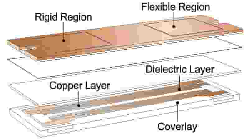
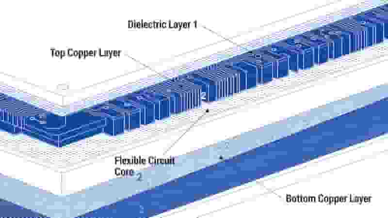
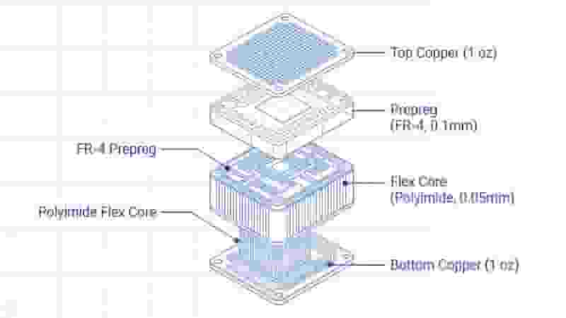
A rigid-flex pcb stackup defines the layered arrangement of conductive copper, dielectric materials, rigid substrates, and flexible substrates in one integrated circuit board. It includes rigid sections (usually FR‑4) and flexible sections (polyimide), bonded and interconnected to form a single reliable unit that supports bending, folding, and 3D packaging.
Key Features of Rigid-Flex PCB Stackup
- Fewer Solder Joints & Connectors: Reduce failure points and improve reliability
- Thinner Profile: Supports compact and lightweight product design
- Better Thermal Performance: Efficient heat dissipation for high-power devices
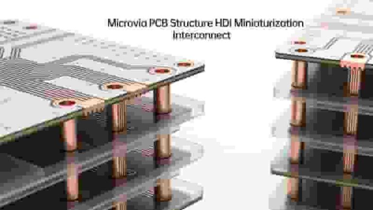
- High-Density Interconnect: Ideal for HDI and complex circuits
- 3D Assembly Capability: Bending and folding for space‑limited products
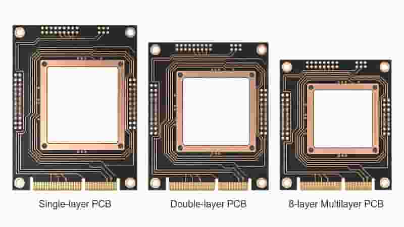
Types of Rigid-Flex PCB Stackup
Different stackup structures match different application requirements:
Single-Sided Rigid-Flex PCB
One conductive layer; cost-effective for simple wearable and small electronics.
Double-Sided Rigid-Flex PCB
Two conductive layers; better routing for moderate-complexity devices.
Multi-Layer Rigid-Flex PCB
4-layer, 6-layer, 8-layer stackups for high‑end aerospace, medical, and 5G equipment.
4-Layer Rigid-Flex PCB Stackup Example
| Layer | Material | Function |
|---|---|---|
| Top Rigid Layer | FR‑4 | Component mounting |
| Flexible Layer 1 | Polyimide | Signal routing |
| Flexible Layer 2 | Polyimide | Signal routing |
| Bottom Rigid Layer | FR‑4 | Connector support |
Other common configurations:
- 6-layer: 2 flex layers + 4 rigid layers
- 6-layer: 4 flex layers + 2 rigid layers
- 8-layer: 4 flex layers (air gap) + 4 rigid layers
- 8-layer: 6 flex layers (air gaps) + 2 rigid layers
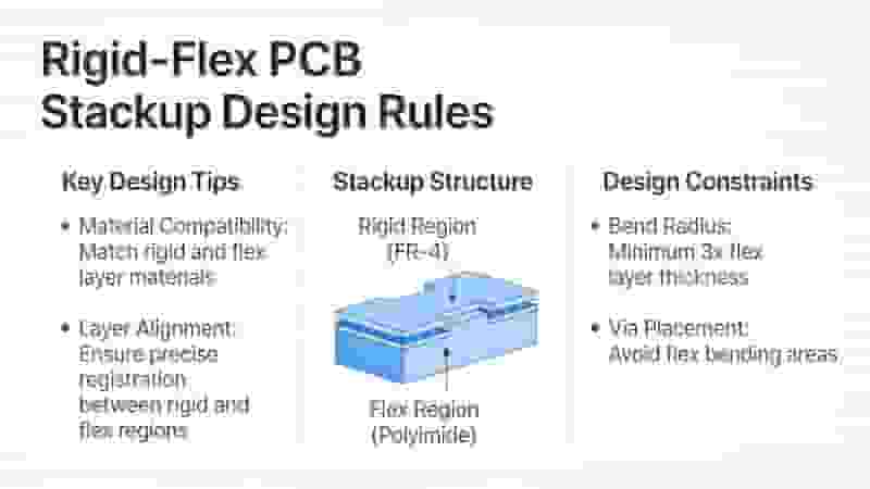
Design Considerations for Rigid-Flex PCB Stackup
Professional design rules to ensure performance and yield of rigid-flex pcb stackup:
- Select high-quality polyimide and FR‑4 materials
- Keep bend radius ≥ 10x flex layer thickness
- Avoid vias in dynamic bending zones
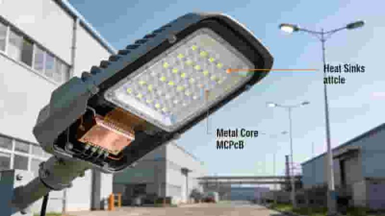
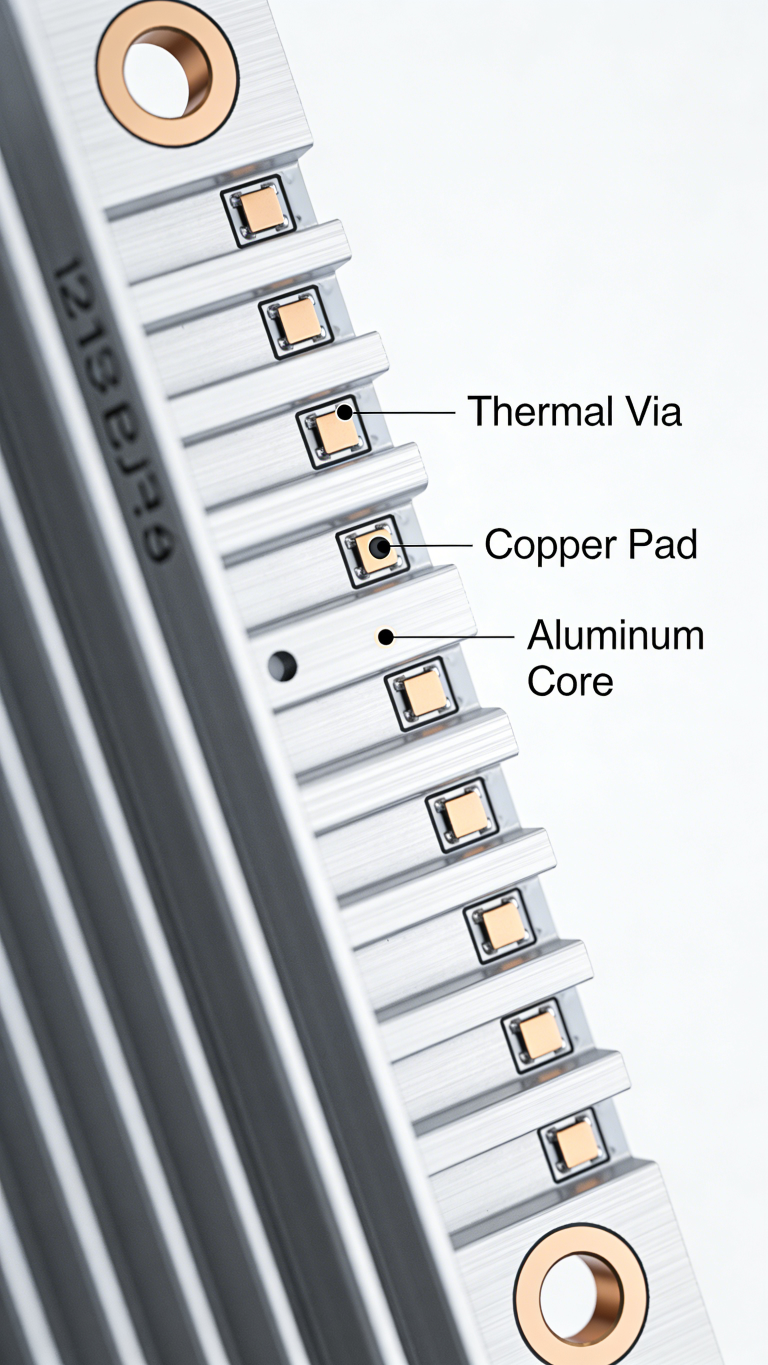
- Use thermal vias for high-power components
- Optimize trace width and spacing for signal integrity
- Follow IPC‑2223 and IPC‑6013 standards
Real-World Applications
Rigid-flex PCBs are widely used in high‑reliability industries:
- Medical Devices: Pacemakers, endoscopic devices, health monitors
- Automotive & EV: ADAS, battery management, in‑vehicle systems
- 5G & IoT: High-frequency antennas, communication modules
- Aerospace: Satellite and avionic control systems
We provided a 6-layer rigid-flex PCB solution for a wearable health monitor, reducing thickness by 30% while ensuring stable signal integrity.
Industry Trends & Insights
The global rigid-flex PCB market grows at a CAGR of 7.5% (2023‑2030), driven by 5G, IoT, foldable screens, and wearable devices. HDI rigid flex pcb stackup has become the mainstream choice for high‑end miniaturized products.
Pro Design Tip: Asymmetric stackup can lower cost while keeping flexibility for 3D assembly.
Get Your Custom Rigid-Flex PCB Stackup Solution
We specialize in rigid-flex PCB design, prototyping, and mass production with optimized stackup, high quality, and on-time delivery. Send your files for a free quote now.
Request Free Quote
How to Build a Multilayer PCB: Full Stack‑Up, Manufacturing & IPC Compliance Guide
SMT PCB Assembly Services for Prototypes & Production
What Is Prototype PCB Assembly
What is a Blank PCB? Buy Bare Circuit Boards | Layer PCB
SMT PCB Assembly Services for Prototypes & Production