This guide explains microvias definition, IPC standards, manufacturing, advantages, and applications to help engineers and buyers evaluate microvia PCB solutions for high-density, miniaturized electronics.
What Are Microvias in PCBs?
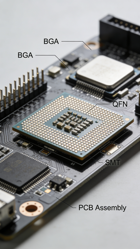
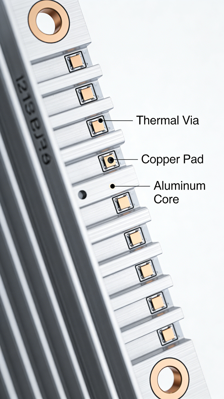
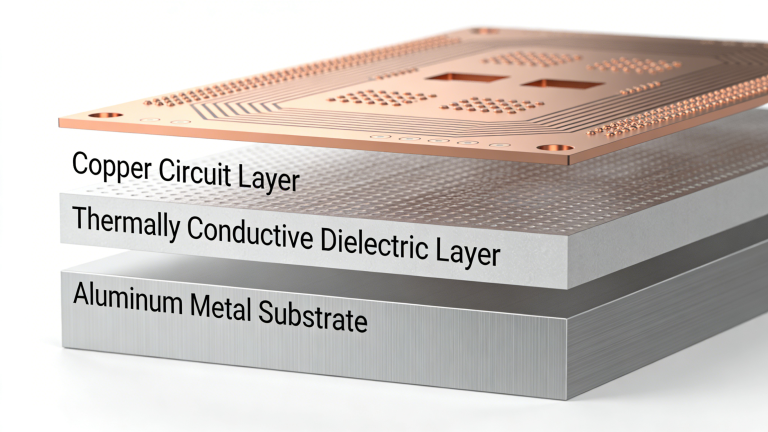
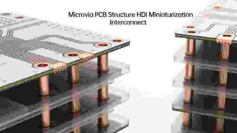
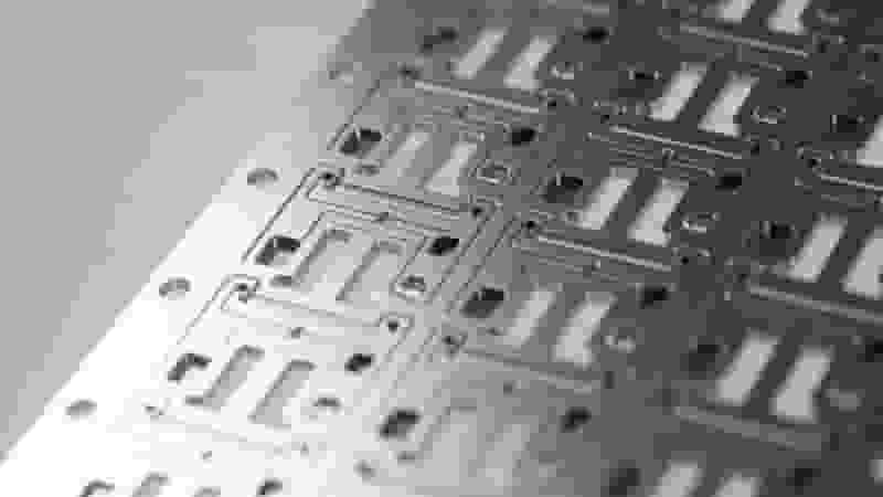
As printed circuit boards are designed to pack more components into increasingly compact spaces, microvias play a crucial role in enabling further miniaturization. Microvias are small, high-precision vertical interconnects used in HDI (High-Density Interconnect) PCBs to connect adjacent layers without drilling through the entire board.
Typically measuring 0.005–0.015 inches (0.13–0.38mm) in diameter, microvias reduce PCB thickness, shrink layer counts, and maximize routing density. They replace traditional through-hole vias (PTH) that consume excessive space and limit miniaturization in modern electronics.
Types of Microvias
There are two primary production technologies for microvias, each optimized for different design requirements:
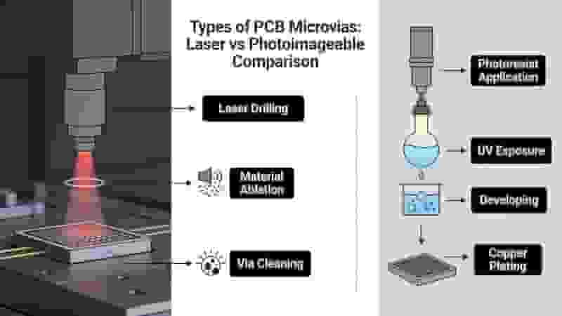
Laser-Drilled Microvias
Laser drilling (CO2, YAG, excimer) creates microvias down to 0.005 inches with high density PCBs precision. Benefits include:
- Small via capture pads and fine annular rings (down to 0.003 inches)
- Aspect ratios up to 15:1 for thick multilayer PCBs
- Ideal for high-density, high-complexity designs
Photoimageable Microvias
UV patterning and copper plating form microvias at lower cost for moderate-density boards. Typical minimum size is 0.006 inches.
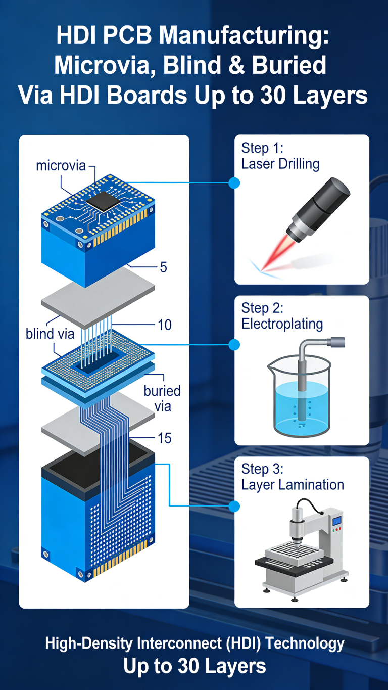
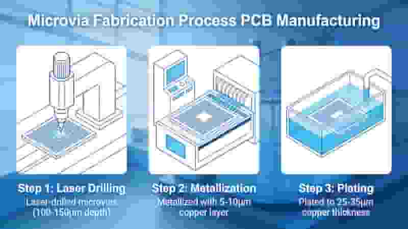
Microvia Fabrication Process
Reliable microvia production requires strict process control across four core stages:
Stacked & Staggered Microvias
- Stacked: Aligned vertically for direct layer connections
- Staggered: Offset layout reduces thermal stress and improves reliability
Precision Laser Drilling
Tight energy control and positioning ensure consistent microvia diameter, depth, and taper.
Metallization & Plating
Electroless copper seed layer + electroplating fill microvias completely without voids.
IPC-Compliant Process Control
Automated optical inspection (AOI) and statistical process control (SPC) maintain microvia quality and yield.
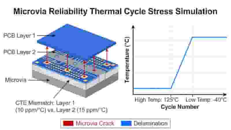
Microvia Reliability Factors
Long-term performance of microvias depends on three critical factors:
- Thermal Cycling: CTE mismatch between copper and laminate causes stress; minimized by optimized microvia design
- Capture Pad Size: Adequate pad area ensures stable microvia bonding during thermal expansion
- Underfill & Encapsulation: Protects microvias from moisture and mechanical stress
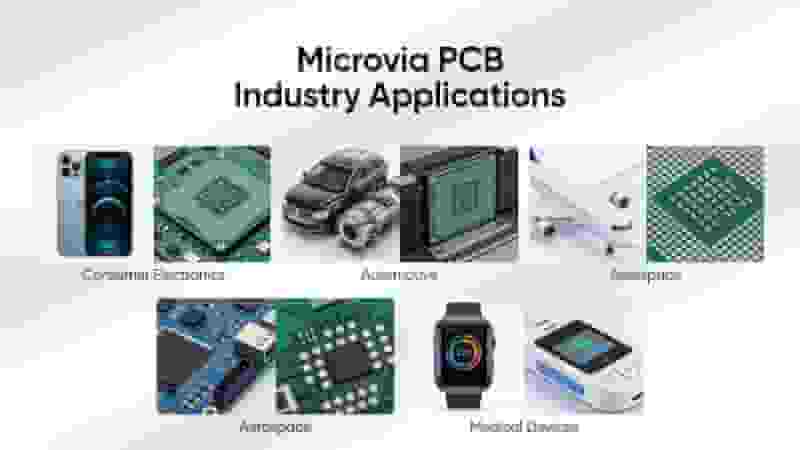
Industry Applications of Microvias
Microvias enable miniaturization in high-reliability sectors:
- Consumer Electronics: Smartphones, wearables, IoT devices
- Automotive: ADAS, infotainment, power electronics
- Aerospace & Defense: Guidance systems, satellite circuits
- Medical Devices: Implants, ultrasound, diagnostic equipment
Future Trends of Microvias
Advancements in laser drilling and plating will shrink microvias further, boost aspect ratios, and improve yields. Microvias will remain foundational for HDI, multilayer PCB, and advanced packaging in AI, 5G, and quantum computing.
Conclusion & Custom Solutions
Microvias are indispensable for modern PCB miniaturization, offering unmatched density, performance, and reliability. We specialize in microvia PCB design, prototyping, and mass production with IPC Class 2/3 standards, fast lead times, and competitive pricing.
Get Your Microvia PCB Solution Today
Contact us for a free DFM review, custom quote, or prototype service for your microvia and HDI PCB projects.
Request a Quote
Solder Paste and Solder Paste Printing in SMT PCB Assembly
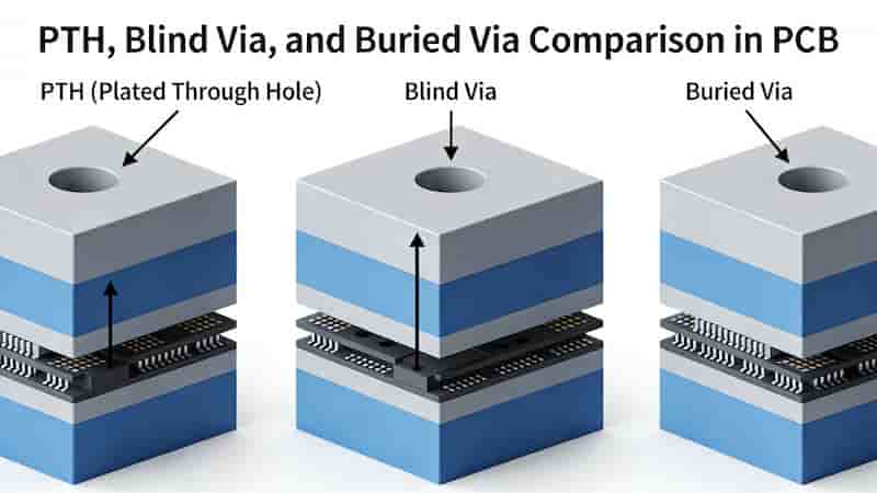
Blind Vias & Buried Vias in PCBs – The Complete Technical Guide
High-Reliability PCBs For New Energy Applications
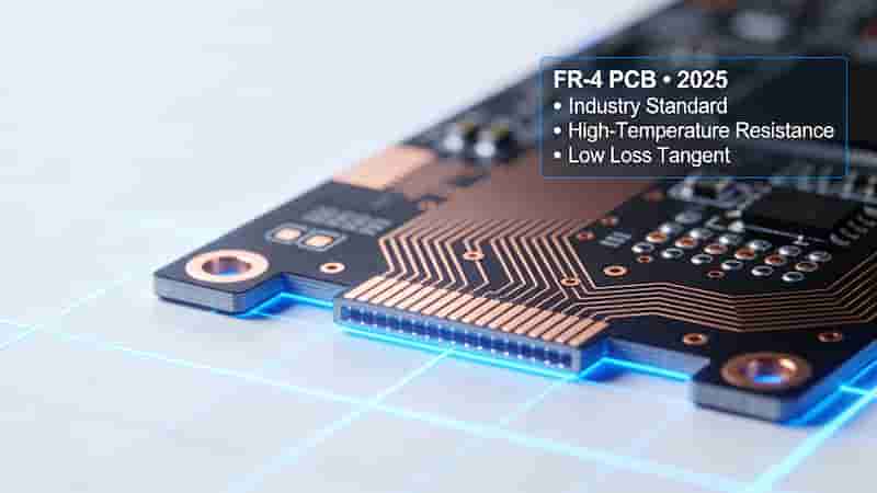
Why Choose FR-4 as Your PCB Material in 2025? The Definitive Guide
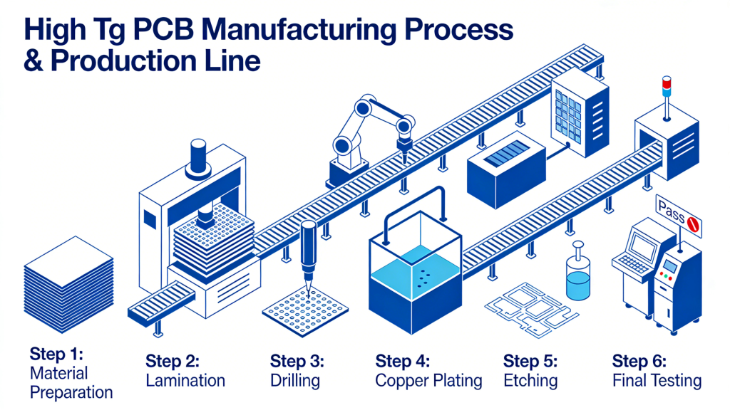
High Tg PCB Manufacturing for High Temperature Applications