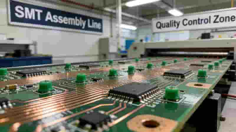
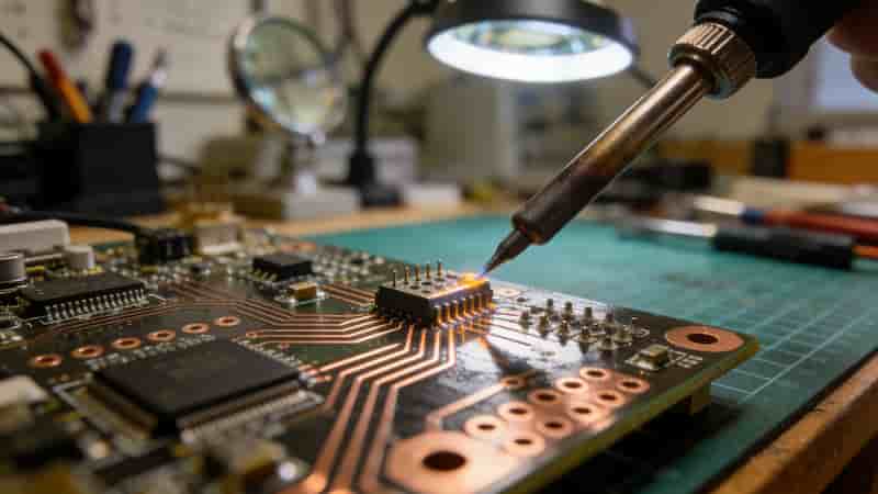
Understanding the key differences between PTH and via is essential for optimizing PCB design and manufacturing. This article defines PTH and via, compares dimensions, functions, locations and finishing requirements. Typical applications and design considerations are also discussed to help engineers and buyers make informed decisions.
Defining PTH and Vias in PCBs
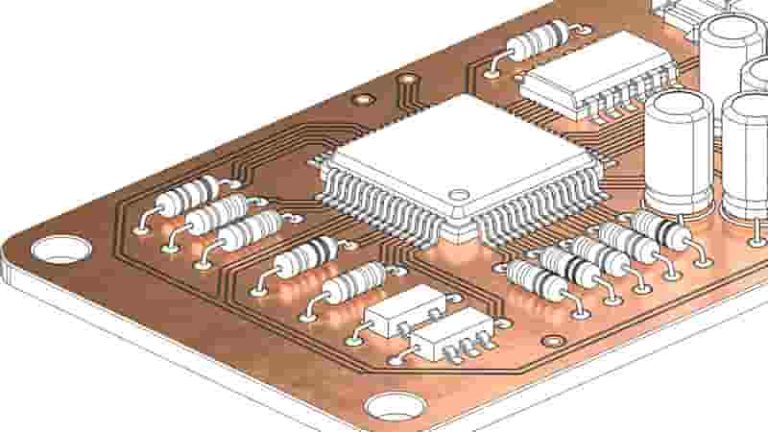
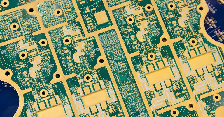
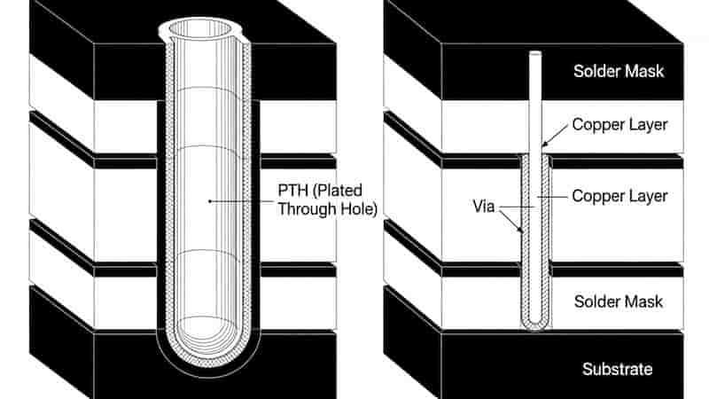
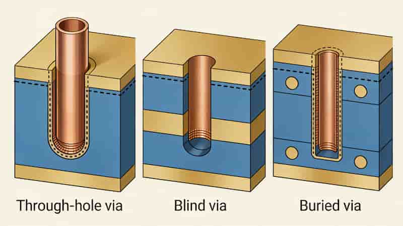
PTHs (Plated Through Holes) are vertical holes that span entire multilayer PCBs and enable conduction between layers. The holes typically have a diameter between 0.15mm to 2mm. The walls of the holes are plated with copper to facilitate electrical connectivity. PTHs primarily function to connect surface mount pads or through hole pads to internal traces and planes, enabling mounting and interconnecting electronic components.
Vias are also vertical interconnects but they are localized connections within or between layers of a PCB. Vias have smaller diameters than PTHs, usually between 0.1mm to 0.5mm. While PTHs function mainly for component connections, vias are primarily used to route signals between traces on different layers, focusing on allowing trace routing rather than component placement.
PTH vs Via – Key Characteristics Comparison
| Feature | PTH (Plated Through Hole) | Via |
|---|---|---|
| Definition | Plated hole through entire PCB | Electrical connection between layers |
| Primary Purpose | Component mounting & layer connection | Signal routing between layers |
| Size Range | 0.15mm – 2mm diameter | 0.1mm – 0.5mm diameter |
| Layer Coverage | Spans all layers | Connects specific layers |
| Component Mounting | Direct component mounting | No direct mounting |
| Finishing | Solder mask & special preparation | Minimal finishing required |
Typical Applications
PTH Applications
- Component lead connections for through-hole devices
- Multi-layer stacking – The spanning nature of PTHs enables connectivity across entire multi-layer PCB stackups, ideal for high-density designs.
- Power and ground plane connections
- EMI shielding and grounding applications
Via Applications
- High-density trace escape routing
- Signal layer translation
- Heat dissipation for SMT components
- Stitching vias for improved conductivity
Design Guidelines for Optimal PCB Fabrication
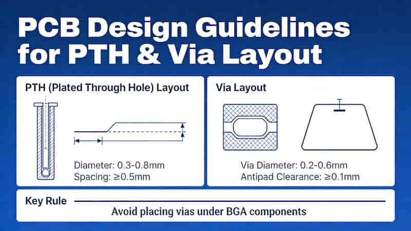
For PTHs: Match hole diameters to component leads, optimize padstack quantity, and provide sufficient thermal reliefs for high-power connections to ensure reliable PCB manufacturing.
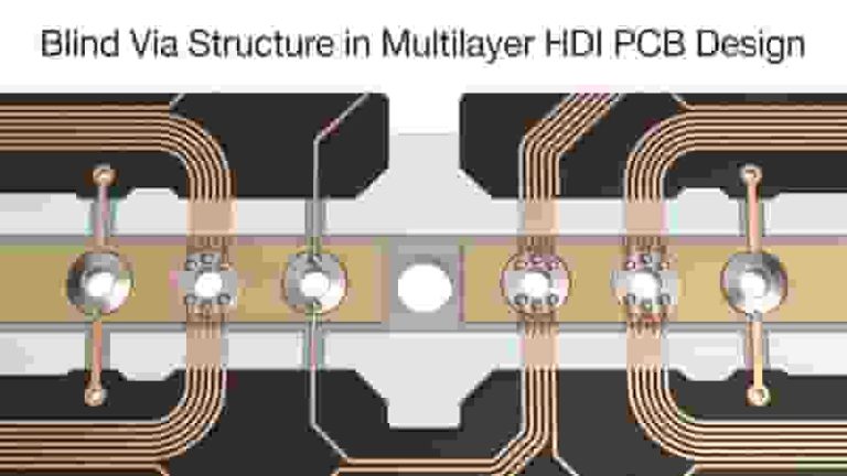
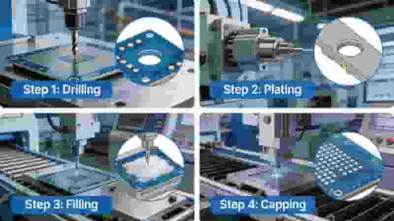
For vias: Verify minimum annular ring requirements, consider signal impedance impact, and ensure proper filling for blind and buried vias to prevent reliability issues in multilayer PCBs.
Conclusion
PTHs and vias both enable vertical conductivity in PCBs but serve distinct purposes. PTHs span entire boards for component mounting, while vias provide localized layer connections for signal routing. Proper application of these interconnects is crucial for optimizing PCB design, performance, and manufacturing yield.
Understanding these differences helps design engineers create more efficient, reliable, and cost-effective PCB solutions for various electronic applications.
Need Professional PCB Manufacturing Services?
We provide high-quality PCB fabrication, prototype development, and full PCB assembly services with strict quality control. Get expert support for your PTH and via design requirements.
Request a free quote or consult our engineering team for your multilayer PCB projects.
Contact Us for a Free Quote
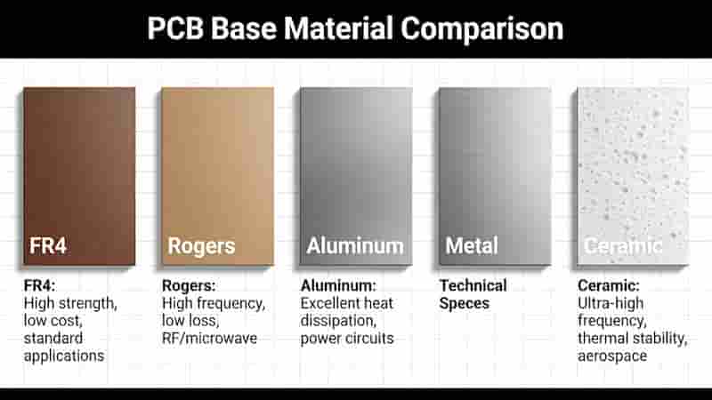
Key Factors Influencing Custom PCB Costs in 2025
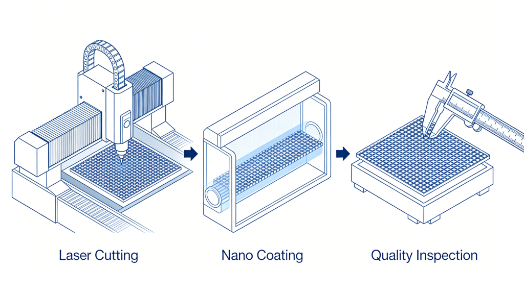
Nano-Coated PCB Stencil Manufacturing for Precision & Durability
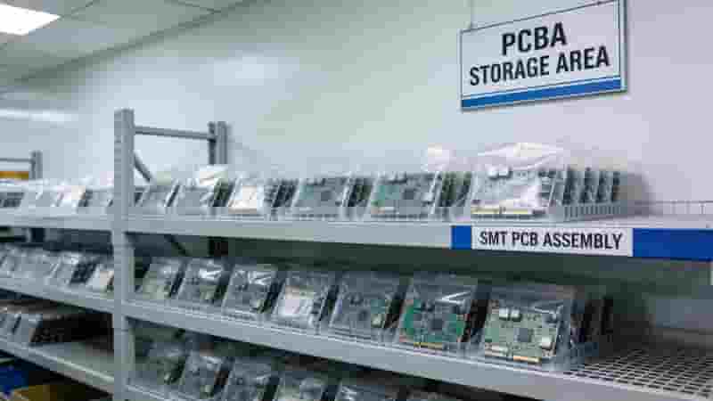
How Long Can PCBA Finished Products Be Stored?
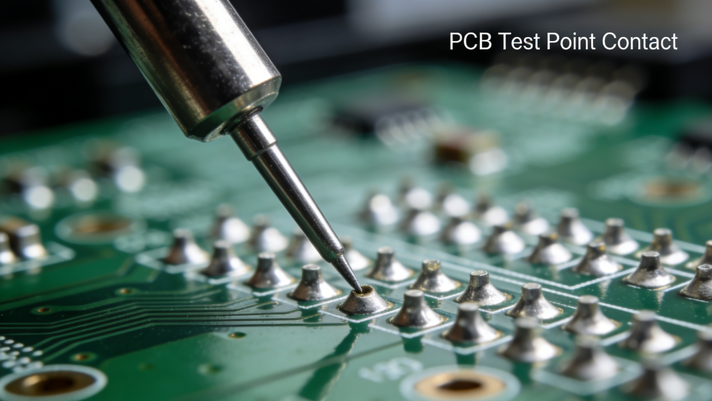
Flying Probe Testing for PCB: The Complete Professional Guide
Rigid-Flex PCB Manufacturing & Prototype Services