Plated half-holes, also called castellated holes, provide a space-efficient way to interconnect separate PCB modules by soldering. Unlike bottom pads, their edge positioning simplifies mounting and enhances reliability. This article explains everything about plated half-hole structures, design guidelines, manufacture, benefits and use cases.
Structure of Plated Half-Holes
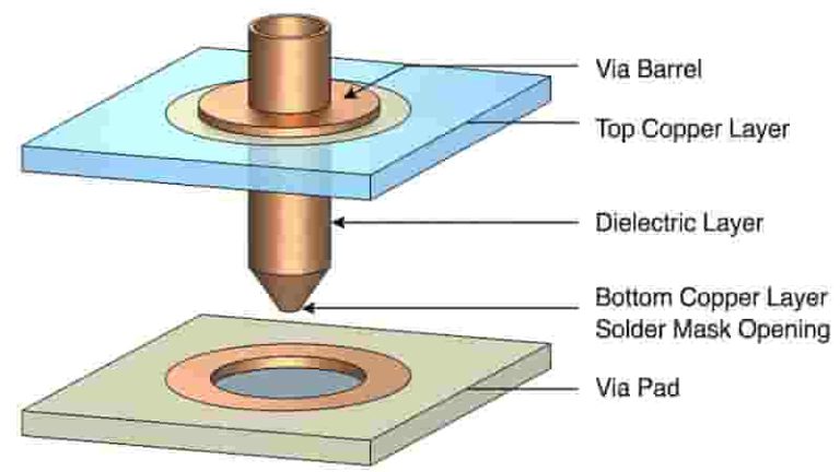
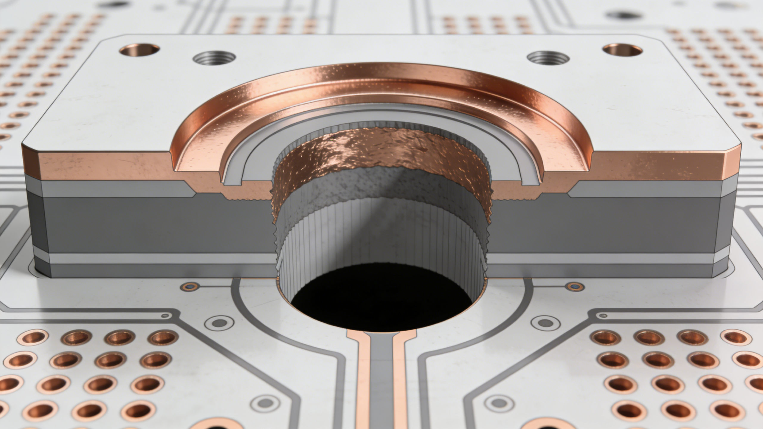
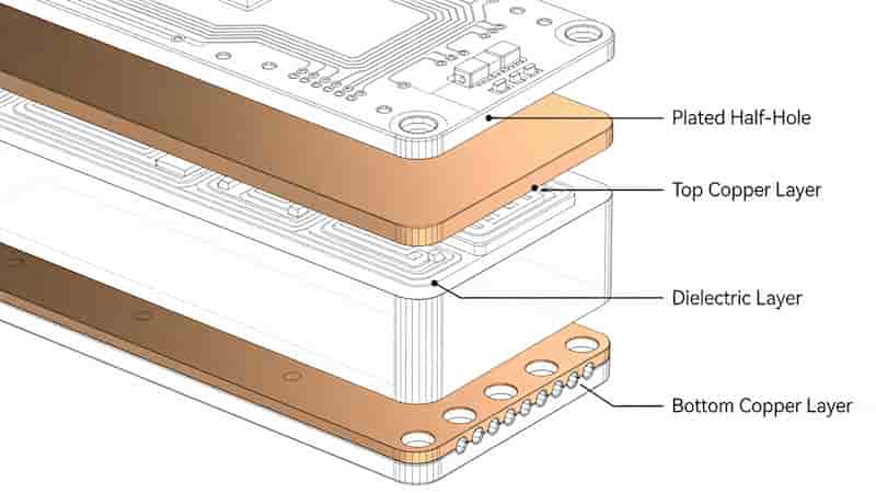
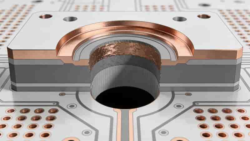
Plated half-holes, also known as castellated holes, resemble plated through-holes in structure but occupy only half the vertical space. As illustrated below, they plate the walls on one side of the hole.
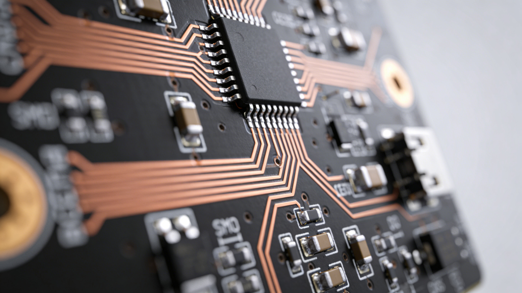
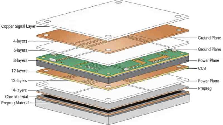
Half-holes connect individual PCB modules to main boards via soldering. Compared to under-module pads, they improve joint access and coaxial alignment. Half-holes also facilitate modular board assembly and high-density interconnects.
Design Guidelines
When designing plated half-holes, consider the following critical factors:
- Position precisely on board edges for easy accessibility
- Define as plated through-holes in EDA tools
- Include in drill files for manufacturer
- Add pads on each layer for stability
- Mind minimum sizing based on board thickness
- Choose half-hole diameters balancing via reliability, routing spaces, and costs
Fabrication Process
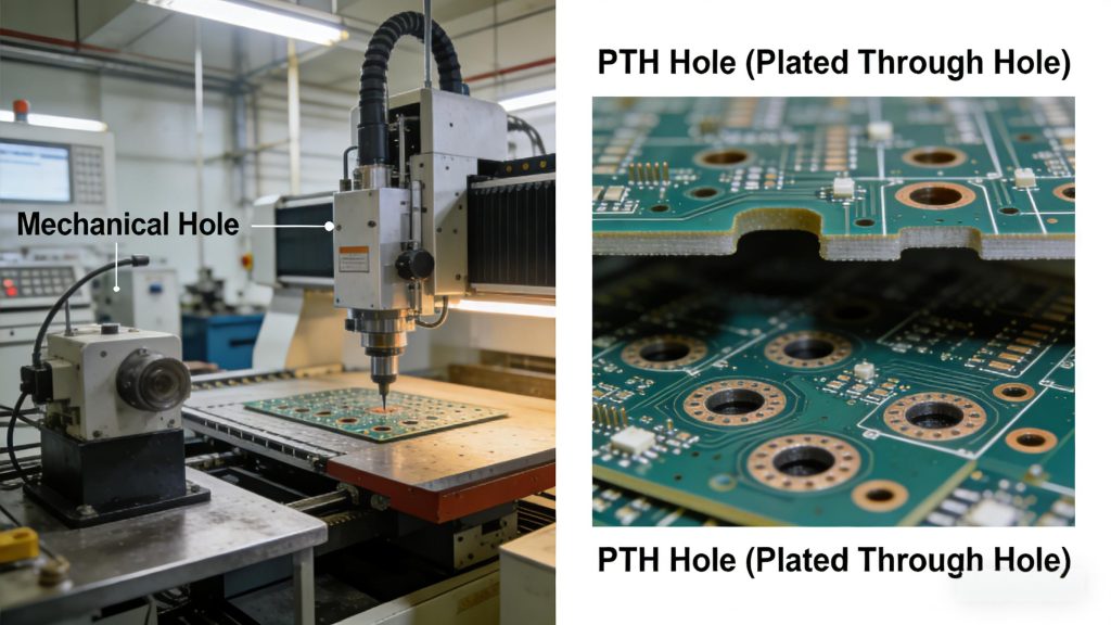
Traditional processes have limitations in productivity and performance. Newer methods utilize specialized drilling on panel edges and direct copper plating to boost efficiency. One-step solutions like precision laser cutting also exist for high-precision castellated holes.
Key Benefits
Half-holes simplify soldering, measurement, and inspection versus bottom-located pads. Their edge positioning enhances coaxiality while avoiding dust traps. Half-holes also reduce via filler challenges and enable flexible routing options for modern PCB designs.
Applications
- Modular boards
- Changing component layouts
- High-density interconnections
- Validating solder joint quality
- Bridging rigid-flex PCB sections
Plated half-holes continue finding increased applications in complex modular PCB designs due to their flexibility and reliability.
Conclusion
Incorporating plated half-holes in suitable designs allows improving interconnect accessibility, manufacturability, and reliability. We hope this overview aids your learning. Please reach out with any questions!
Need Custom Plated Half-Hole PCBs?
We provide professional PCB manufacturing, DFM analysis, and reliable assembly for castellated hole modules. Get a free quote today.
Contact Us for a Quote
Turnkey PCB Manufacturing and Assembly: Full One-Stop Solution Advantages
Double-sided PCB Manufacturing Process – We Deliver Compliant, Efficient Production
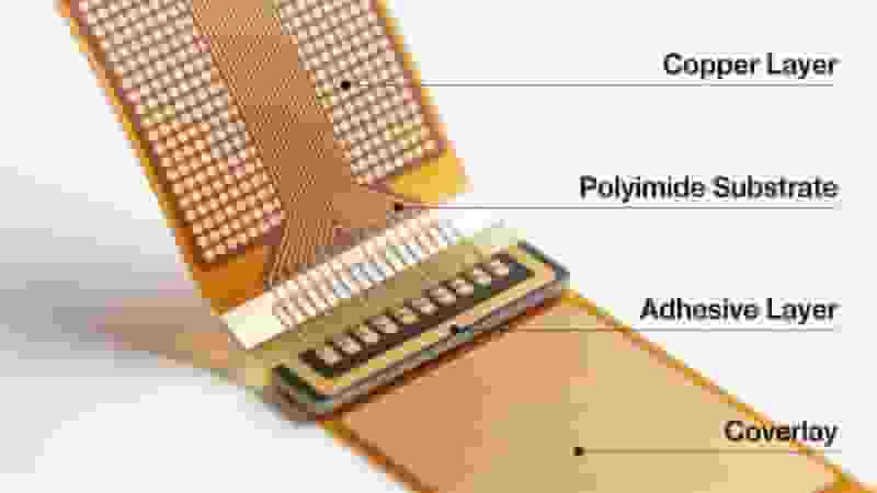
Complete Introduction of Flexible Circuit Board Materials
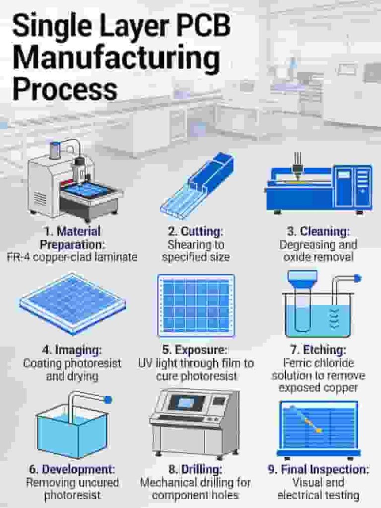
Single Layer PCB Manufacturing | Affordable Single Sided PCBs
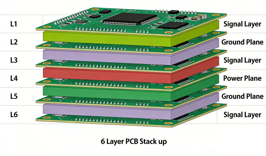
6 Layer PCB Guide: Stackup, Thickness, Design & Competitive Price