How to Convert Circuit Diagram to PCB Layout: A Complete Guide
Discover the essential steps to convert circuit diagrams into optimized PCB layouts. We share professional insights on tools, common pitfalls, and advanced techniques to ensure your designs are manufacturable and high-performing. Ideal for engineers seeking reliable PCB prototype and assembly services.
In the fast-paced world of electronics, turning a conceptual circuit diagram into a functional PCB layout is the bridge between innovation and real-world application. With over a decade of experience in PCB manufacturing, we’ve seen countless designs evolve from simple sketches to high-performance boards used in automotive, medical, and consumer electronics.
Whether you’re a hobbyist or an engineer, understanding how to convert circuit diagram to PCB layout is essential. This guide walks you through the full process with expert insights, from schematic design to Gerber file generation, to ensure your PCB is reliable, efficient, and ready for fabrication.
Why Converting Circuit Diagrams to PCB Layouts Matters
A poorly executed conversion leads to signal integrity issues, thermal problems, or manufacturing defects. A well-optimized PCB layout improves performance, reduces waste, and speeds up time-to-market. Proper planning can reduce rework by up to 50%.
Step-by-Step Process: How to Convert Circuit Diagram to PCB Layout
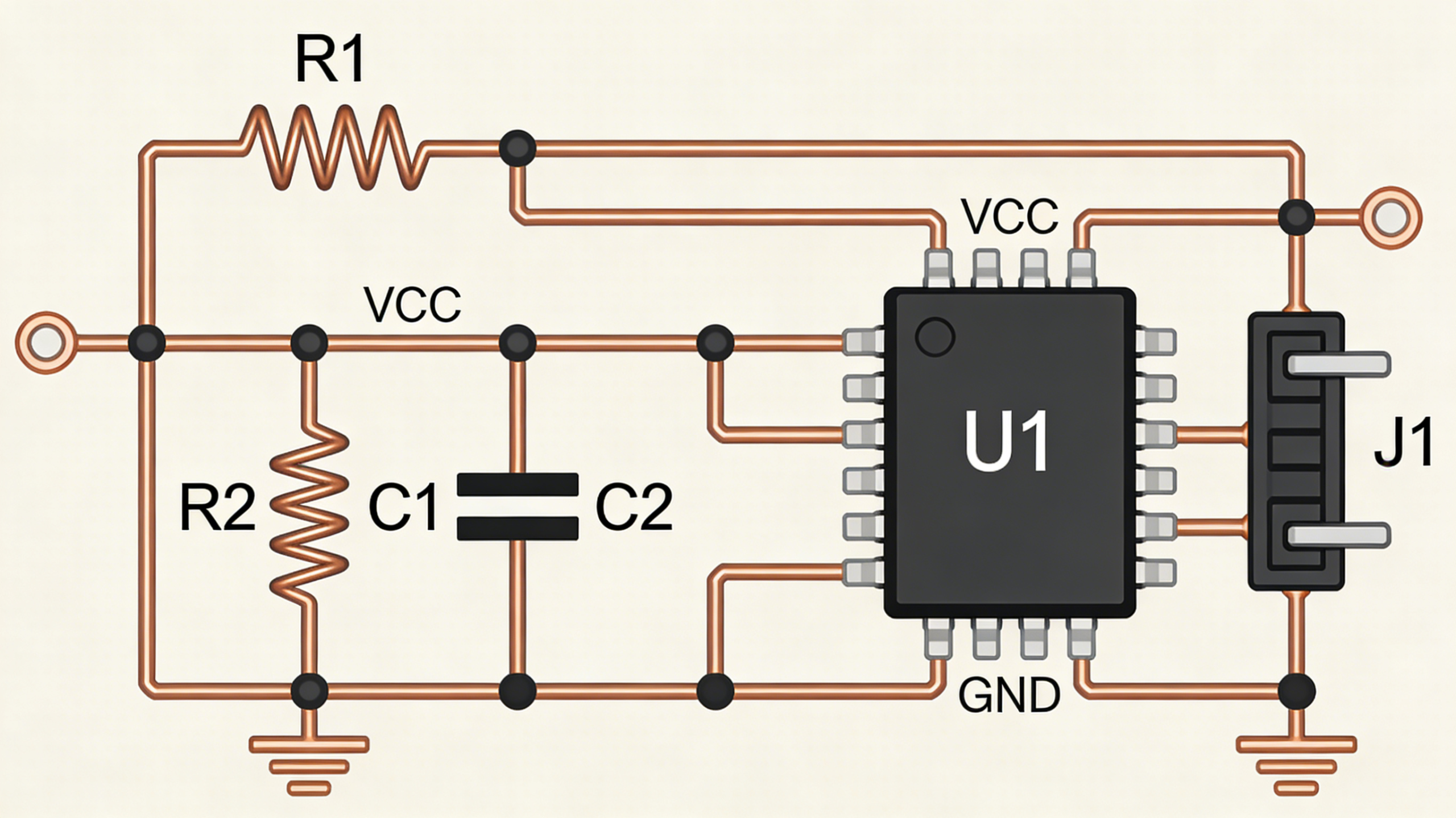
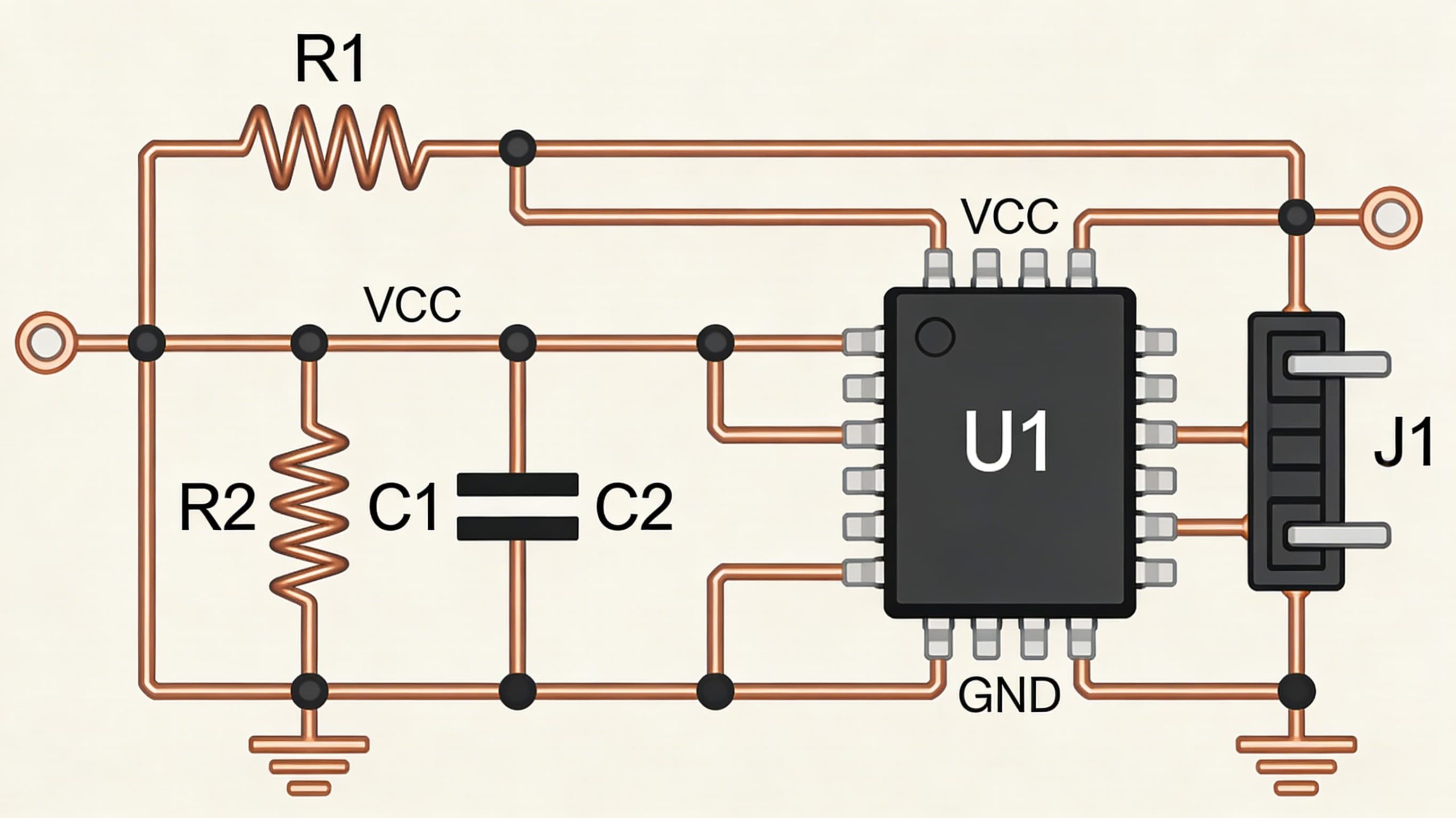
1. Circuit Schematic Design
Start with a complete schematic using Altium Designer, KiCad, OrCAD, or Eagle. Define components, connections, and run simulations to verify functionality.
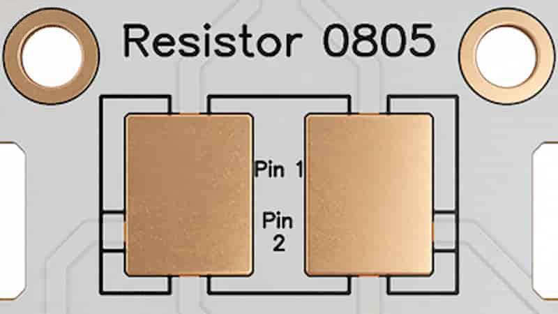
2. Component Footprint Assignment
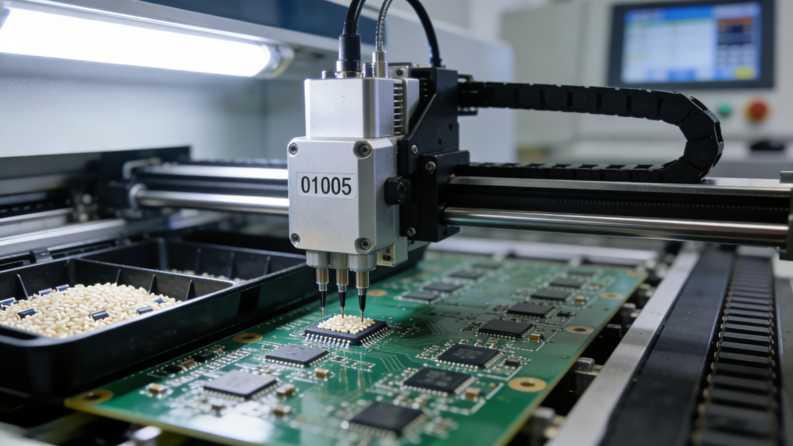
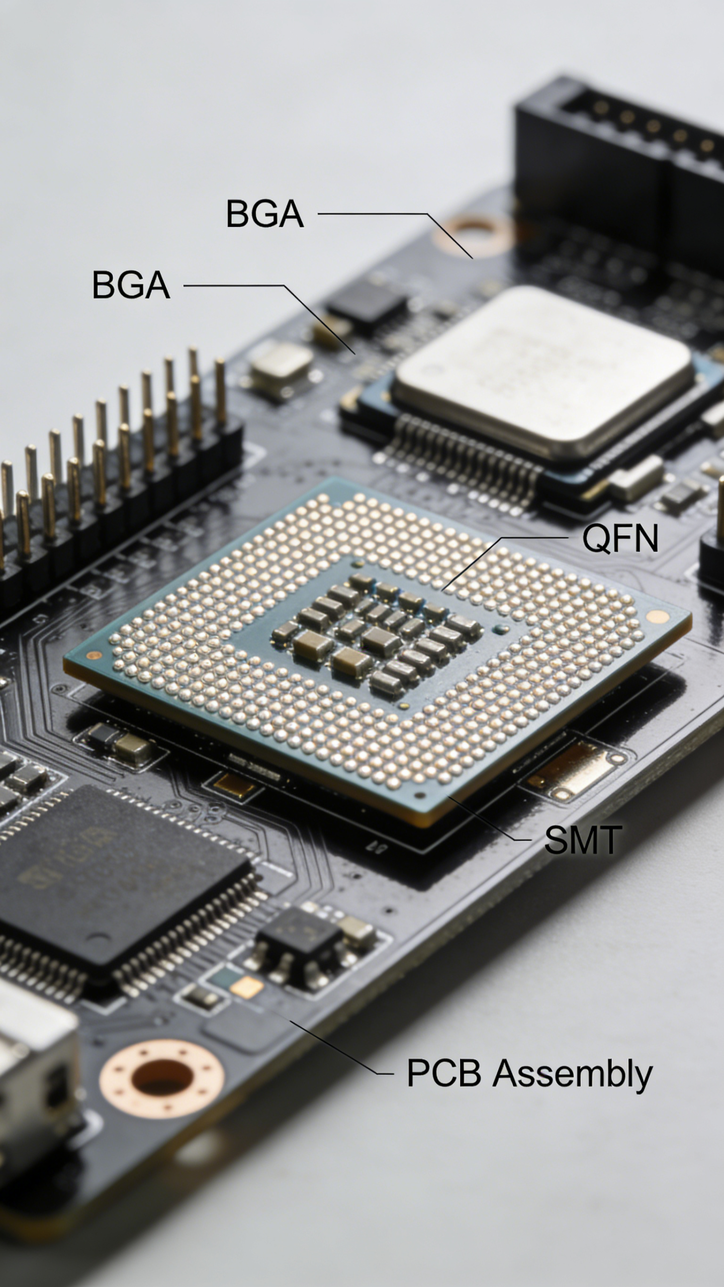
Assign physical footprints based on manufacturer specs. Follow JEDEC standards for SMT components to ensure assembly compatibility.
3. PCB Outline Creation
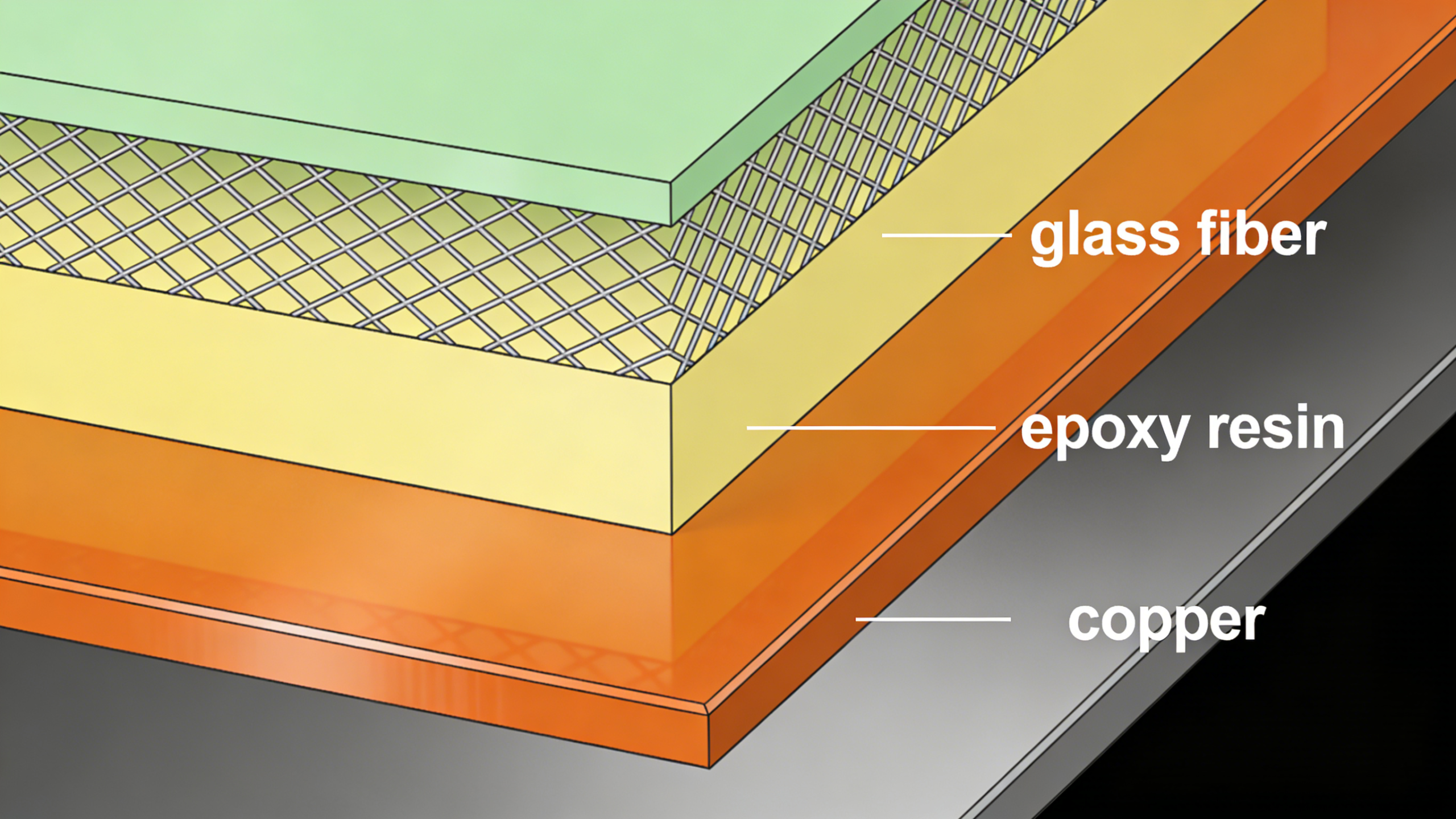
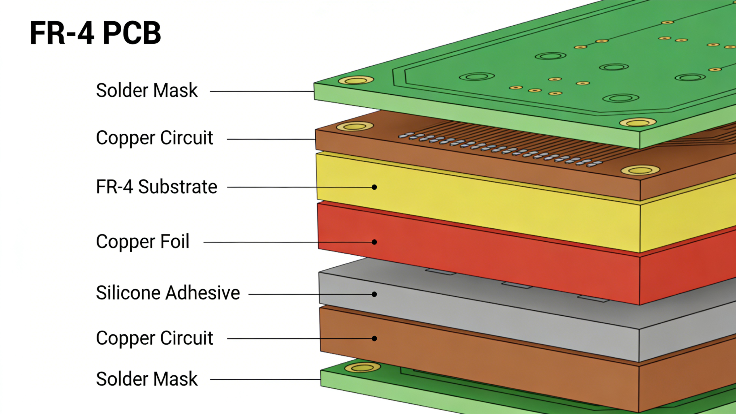
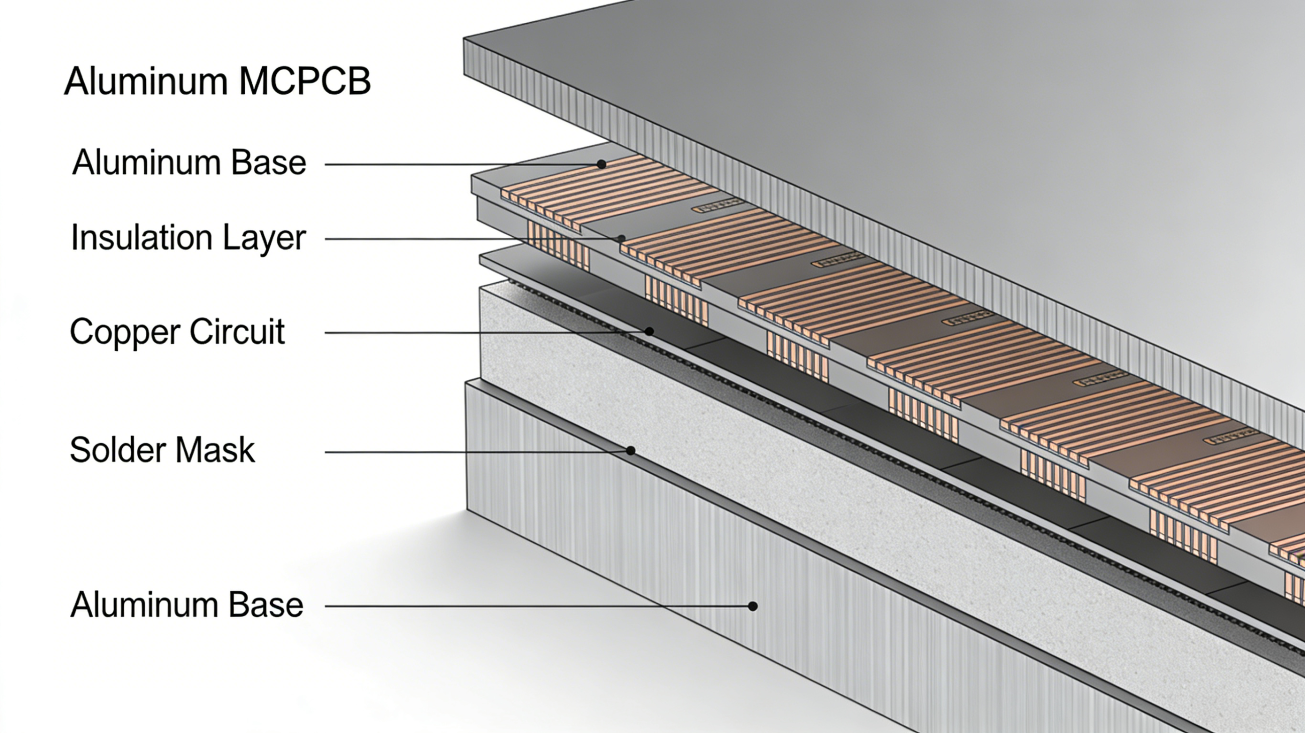
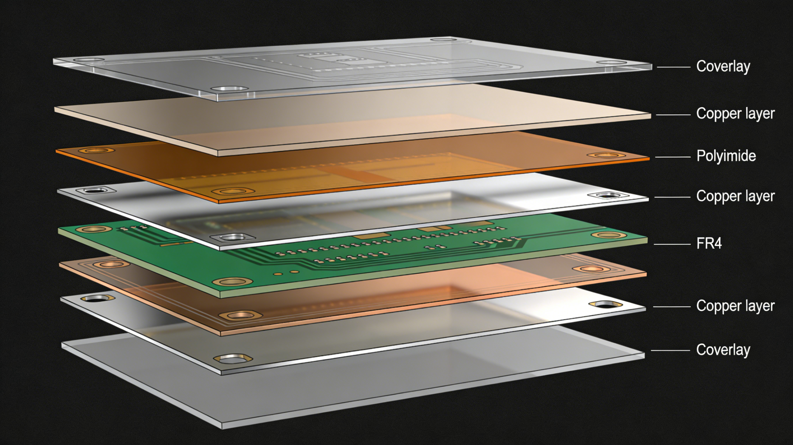
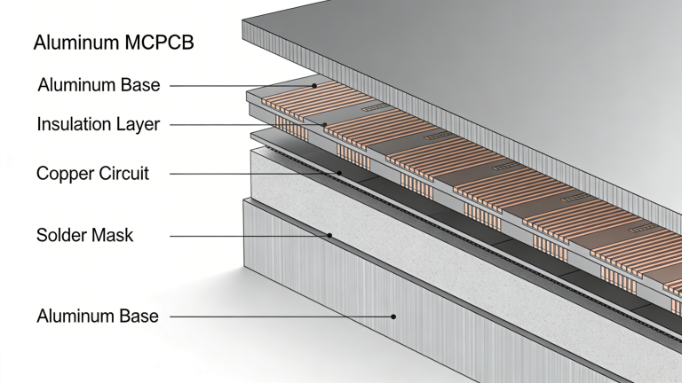
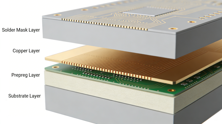
Define board shape, size, mounting holes, and layer stackup. Choose single-sided, double-sided, or multilayer based on your design needs.
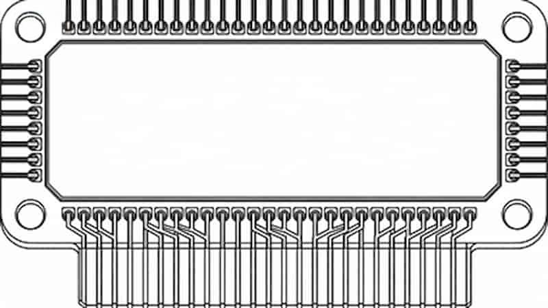
4. Component Placement
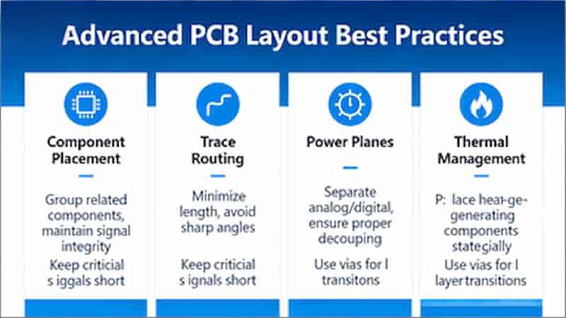
Place components to minimize trace length, reduce noise, and improve thermal management. Separate analog and digital sections for best performance.
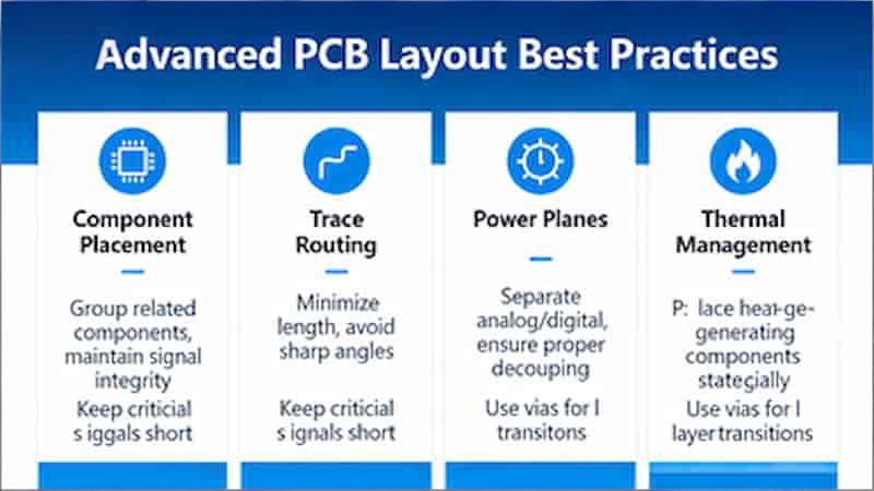
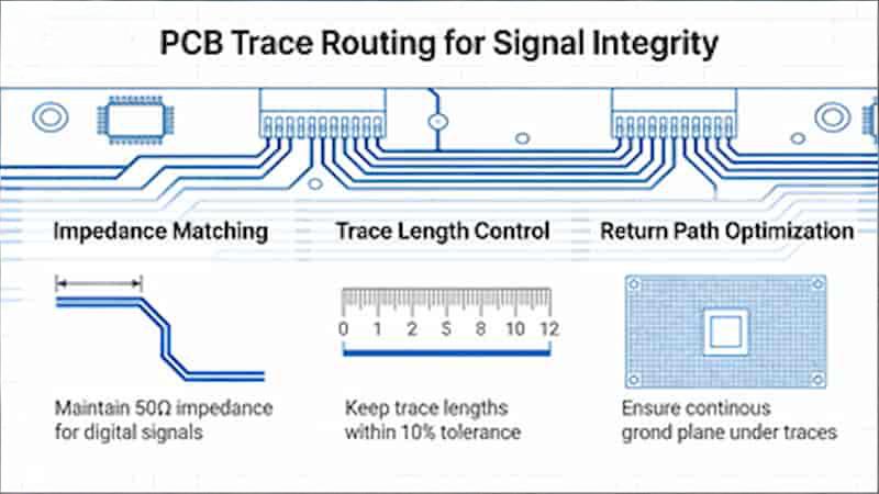
5. Trace Routing
Route copper traces using IPC standards. Use 45-degree angles, avoid stubs, and match lengths for high-speed signals like USB and HDMI.
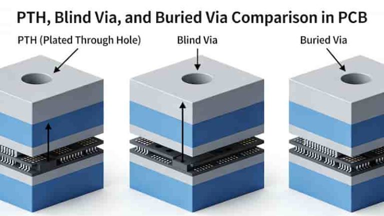
6. Vias and Power/Ground Planes
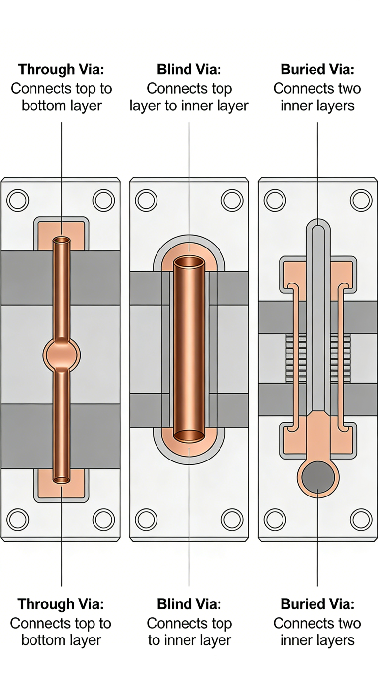
Add vias for multilayer boards and use solid power/ground planes to reduce EMI and improve stability.
7. DRC & ERC Check
Run Design Rule Check and Electrical Rule Check to fix errors before production.
8. Gerber File Generation
Export Gerber files, drill files, and documentation for PCB manufacturing.
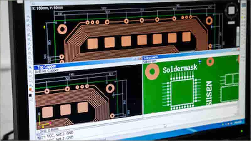
Circuit Diagram to PCB Layout: Process Overview
| Step | Process Stage | Key Actions | Common Tools / Standards |
|---|---|---|---|
| 1 | Schematic Design | Create complete circuit diagram, define components and connections | Altium Designer, KiCad, OrCAD, Eagle |
| 2 | Footprint Assignment | Assign physical footprints per manufacturer specs | JEDEC standards for SMT |
| 3 | PCB Outline Creation | Define board shape, size, mounting holes, layer stackup | Single/double/multilayer selection |
| 4 | Component Placement | Optimize positions for thermal, signal, and assembly requirements | Analog/digital separation |
| 5 | Trace Routing | Route copper traces with proper width, angle, and length | IPC standards, 45-degree angles |
| 6 | Vias & Power Planes | Add vias and solid power/ground planes | EMI reduction techniques |
| 7 | DRC & ERC Check | Run design and electrical rule checks | Built-in EDA tool checkers |
| 8 | Gerber File Generation | Export manufacturing files and documentation | Gerber RS-274X, Excellon drill |
Advanced Tips for Flawless PCB Layouts
- Run signal integrity simulation
- Confirm component availability early
- Use lead-free materials
- Add test points for assembly
- Always prototype before mass production
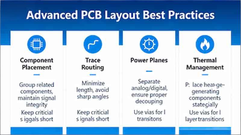
Common Pitfalls to Avoid
Avoid overcrowding, poor thermal design, insufficient clearances, missing DFM rules, and ignored impedance control. These errors cause yield loss and performance failures.
Conclusion
Mastering how to convert circuit diagram to PCB layout turns ideas into reliable products. We provide full-service PCB solutions including prototypes, multilayer boards, rigid, flexible, rigid-flex, SMT assembly, and turnkey manufacturing.
Need Professional PCB Manufacturing & Assembly?
We support global engineers with high-quality PCB prototypes, mass production, and full assembly services. Contact us today for a free quote.