Multilayer PCB stackup and thickness design directly determines signal integrity, EMC performance, impedance control and mechanical reliability of high-speed electronic products. This guide covers standard stackup structures, typical thickness values, and professional selection tips from 4-layer to 14-layer PCBs for industrial and export-grade applications.
Why Multilayer PCB Stackup And Thickness Matter
In modern electronics, products are becoming smaller, lighter, faster and more integrated, yet they are expected to deliver more functionality, higher reliability and a longer service life. To meet these demands, designers increasingly rely on multilayer PCBs, where the layer stackup and overall board thickness play a critical role in the final performance of the product.
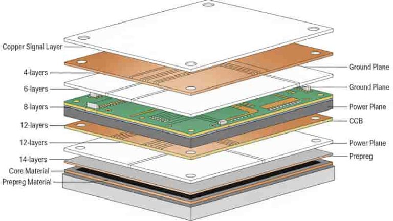
A PCB stackup describes the arrangement of copper layers and insulating layers in the board before layout starts. For a multilayer PCB, this usually includes signal layers, ground planes (GND planes) and power planes (PWR planes), separated and bonded together by core materials and prepregs. Beyond simply deciding how many layers you need, you must also carefully plan which layers carry which signals, how reference planes are placed, and how thick each dielectric layer should be.
A well‑designed multilayer PCB stackup can significantly improve EMC/EMI performance, signal integrity and power integrity, while also helping to control impedance, crosstalk and noise. At the same time, the overall multilayer PCB thickness affects mechanical strength, connector compatibility, thermal performance and manufacturability. On the other hand, a poor stackup choice may lead to excessive EMI radiation, reflections, ringing and reliability issues, even if the schematic and layout rules look correct.
PCB Stackup Basics: Core, Prepreg And Copper Layers
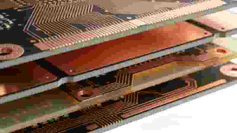
A multilayer PCB stackup is much more than a simple count of copper layers – it is a carefully engineered sequence of copper and dielectric layers that determines how well your board can carry signals, distribute power and withstand mechanical stress. Before the PCB layout begins, the stackup defines where signal layers, ground planes and power planes will be placed, as well as what materials and thicknesses will be used between them.
In a typical multilayer PCB, the main building blocks of the stackup are copper foils, core materials and prepregs. Core is a rigid, copper‑clad laminate (for example FR‑4) that already has copper on both sides and provides the mechanical backbone of the board. Prepreg is a fiberglass fabric pre‑impregnated with resin, used to bond layers together during lamination and to build up the required dielectric thickness between copper layers.
For most designs, a good stackup aims to keep the structure as symmetrical as possible around the center of the board. Symmetrical or “balanced” stackups help reduce warpage and internal stress, especially for high‑layer‑count or large‑size boards.
Key Factors That Affect Multilayer PCB Thickness
The final multilayer PCB thickness is determined by seven critical factors that balance electrical performance, mechanical requirements and manufacturing feasibility:
- Number of Layers and Layer Arrangement: More layers increase total thickness; reference planes add minimum dielectric spacing.
- Core and Prepreg Thickness Selection: The largest contributor to board thickness; varies by material type (1080, 2116, 7628).
- Copper Thickness (Copper Weight): 1 oz vs 2 oz copper directly adds to overall height and impacts impedance targets.
- Impedance Control and High‑Speed Requirements: Dielectric thickness is adjusted to hit 50Ω single-ended or 100Ω differential targets.
- Mechanical Strength and System Constraints: Must match connector specs, enclosure limits, and stiffness needs.
- Thermal Performance and Reliability: Thicker boards improve heat dissipation but affect thermal gradients.
- Manufacturing Capabilities and Cost: Standard thicknesses deliver better yield, cost and lead time.
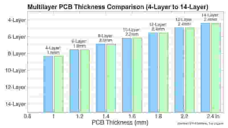
Standard Multilayer PCB Thickness Options (4‑Layer To 14‑Layer)

| Layer Count | Typical Standard Thickness | Common Range | Typical Applications |
|---|---|---|---|
| 4‑Layer PCB | 1.6 mm (0.063″) | ~1.0–2.4 mm | Compact controllers, consumer & industrial boards |
| 6‑Layer PCB | 1.6 mm | ~1.6–2.4 mm | High‑speed digital, MCU + interfaces, control |
| 8‑Layer PCB | 2.0 mm (0.079″) | ~1.6–3.0 mm | Complex high‑speed, telecom, dense FPGA/BGA |
| 10‑Layer PCB | ≈2.0–2.4 mm | ~1.8–3.0 mm | Advanced networking, computing, backplanes |
| 12‑Layer PCB | ≈2.0–2.4 mm | ~2.0–3.0 mm | High‑density, multi‑interface embedded systems |
| 14‑Layer PCB | ≈2.4–3.0 mm | ~2.0–3.2 mm | Very high‑speed, multi‑plane, complex SoC/FPGA |
4‑Layer PCB Stackup And Standard Thickness Options
The 4-layer PCB stackup is the most widely used configuration for embedded systems, industrial controls and consumer electronics. The industry standard thickness is 1.6 mm, with available options from 0.8 mm to 3.0 mm.
Standard 4-Layer Structure:
L1: Top Signal
L2: GND Plane
L3: PWR Plane
L4: Bottom Signal
This structure provides excellent EMI shielding and impedance control while keeping cost low.
6‑Layer PCB Stackup And Standard Thickness Options
A 6-layer PCB stackup adds routing capacity and EMC performance over 4-layer boards. Standard thickness remains 1.6 mm for general use, with 2.0–2.4 mm for high-speed designs.
Recommended 6-Layer Structure:
L1: High-Speed Signal
L2: GND Plane
L3: PWR Plane
L4: Inner Signal
L5: GND Plane
L6: Bottom Signal
Ideal for designs with USB 3.x, PCIe, DDR, HDMI and dense BGAs.
8‑Layer PCB Stackup Overview And Standard Thickness
The 8-layer PCB stackup supports complex high-speed systems with multiple power domains. Standard thickness ranges from 1.6 mm to 2.4 mm, with 2.0 mm being most common.
Symmetrical layer arrangement and multiple ground planes deliver superior signal integrity and EMC performance for telecom and industrial equipment.
10‑Layer PCB Stackup Overview And Standard Thickness
A 10-layer PCB stackup provides abundant routing layers and dedicated planes for advanced systems. Standard thickness is 2.0–2.4 mm to balance density and manufacturability.
Widely used in networking, servers, automotive ECUs and high-performance embedded systems requiring strict impedance control.
12‑Layer PCB Stackup Overview And Standard Thickness
The 12-layer PCB stackup serves very high-density, high-speed designs. Standard thickness falls between 2.0 mm and 2.4 mm using thin dielectric materials.
Multiple ground planes isolate noise between digital, analog and RF sections in 5G, aerospace and medical equipment.
14‑Layer PCB Stackup Overview And Standard Thickness
A 14-layer PCB stackup is engineered for ultra-high-speed, high-complexity systems. Standard thickness is 2.4–3.0 mm to accommodate many layers while maintaining stability.
Used in core network equipment, data center hardware, high-end computing and radar systems.
How To Choose The Right Multilayer PCB Stackup And Thickness
Follow this 7-step process to select the optimal multilayer PCB stackup and thickness:
- Define system interfaces, speed, power and mechanical constraints
- Select initial layer count (4/6/8/10/12/14)
- Confirm controlled impedance requirements
- Choose standard board thickness (0.8/1.0/1.2/1.6/2.0 mm)
- Create symmetrical preliminary stackup
- Validate core/prepreg and impedance with manufacturer
- Document final stackup in fabrication files
Get Custom Multilayer PCB Stackup & Quotation
Need professional multilayer PCB stackup design, impedance control, or accurate thickness customization?
Our engineering team provides free stackup review, DFM analysis and competitive quotes for 4–14 layer PCBs for global industrial buyers.
Request Free Stackup Proposal & Quote
Published for industrial engineers, procurement teams and global electronics manufacturers. All content about multilayer PCB thickness and stackup design is based on industry standards and manufacturing best practices.
Rigid PCB – Single-Sided, Double-Sided & Multilayer

Gold Finger PCB Fabrication & Manufacturing Service
Copper Core PCB vs. Metal Core PCB: Key Differences & Advantages

LED Grow Light PCB: Custom Aluminum PCB & Assembly for Horticulture Lighting
How to Test a PCB for Short Circuit: Complete Professional Guide