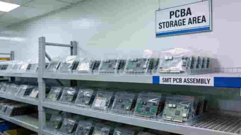
Flying Probe Testing for PCB is a fixtureless electrical test method ideal for low-volume production and prototype circuit boards. Top EMS providers and PCB assembly manufacturers use this advanced technology to ensure high-quality products. Complex PCB circuits often have hidden defects such as short circuits, open circuits, diode faults, and bad solder connections. These issues cannot be seen by the naked eye, so manual inspection is not enough. Flying Probe Testing has become a necessary quality control process.
What is Flying Probe Testing?
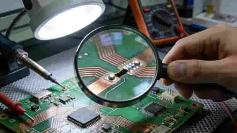
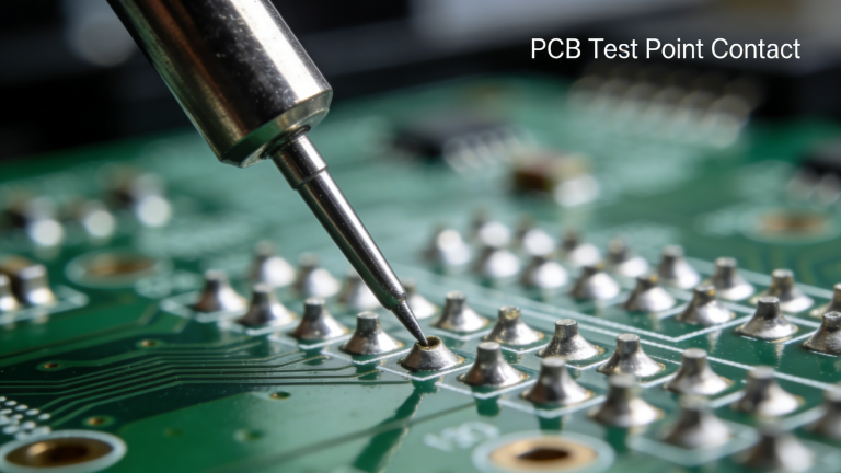
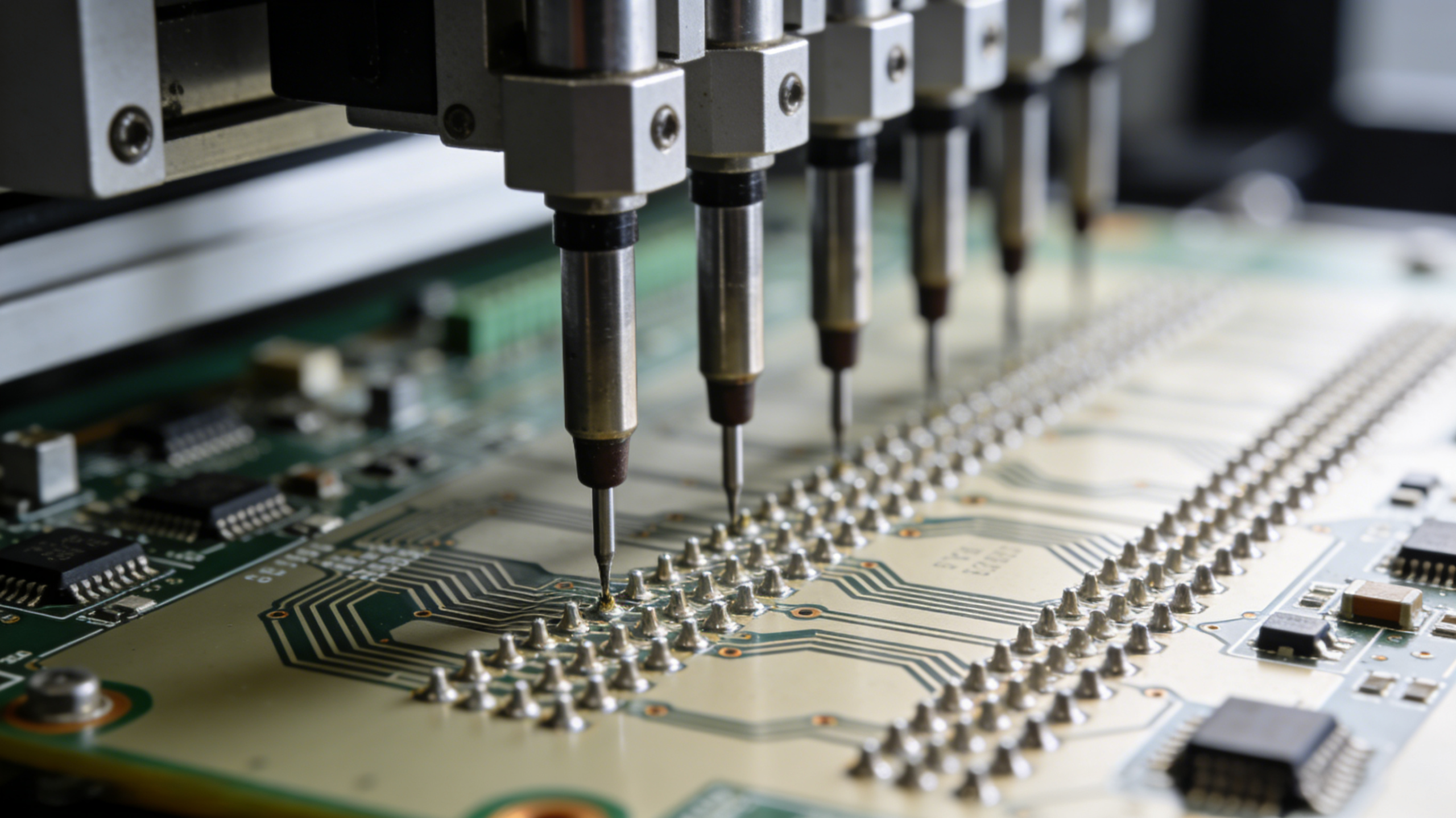
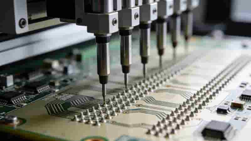
Flying Probe Testing is an electrical test where multiple precision probes move from one node or pad to another to inspect PCBs and PCBA. The independent moving probes look like they are flying over the board surface, which gives this test its name. Initially used only for bare PCBs, upgraded Flying Probe Testing for PCB now supports both bare boards and fully assembled boards.
It can reliably detect short circuits, open circuits, wrong component placement, reverse polarity, and functional failures that are invisible to manual inspection.
Flying Probe Testing vs. ICT Testing
ICT (In-circuit Testing) tests PCBs by contacting test points with fixed pins, but it needs a custom fixture called a bed of nails. This fixture has many fixed pins and requires high upfront cost and long production time.
In contrast, Flying Probe Testing for PCB needs no fixture at all. It uses movable probes to complete all electrical tests, so it is also called fixtureless ICT. This makes it extremely suitable for prototype and low-volume PCB projects.
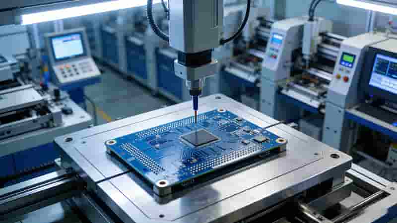
How Does Flying Probe Tester Work?
The working principle is similar to using a multimeter to check component values and measure resistance. Probes check every test point to verify electrical performance and component integrity.
1. Create a test program with full PCB design, component data, and test point coordinates.
2. Load the program into the flying probe tester and place the PCB on the testing platform.
3. The system applies electrical signals, collects real-time data, and compares it with standard parameters.
4. The tester automatically judges defects and generates a complete test report.
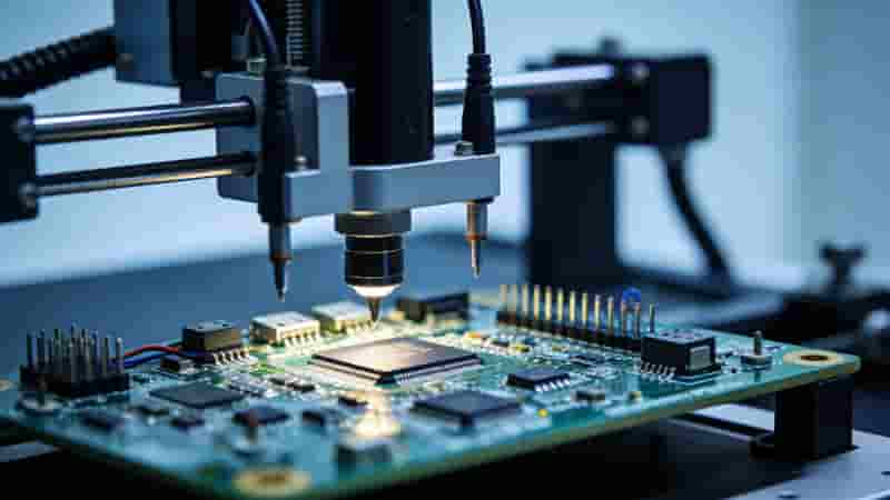
Flying Probe Test for PCBA
Flying Probe Testing for PCB works for both bare boards and assembled PCBs. For bare boards, it checks resistance between circuits to find short and open circuits. For assembled PCBs, it uses multiple electrical signals to verify component values, placement accuracy, and polarity.
This test ensures that both bare printed circuit boards and finished PCB assemblies meet international quality standards.
Advantages and Disadvantages
Advantages
- No Fixture Required – No expensive custom tooling cost
- Cost-Effective – Perfect for small and medium production volume
- Comprehensive Defect Detection – Finds various electrical and assembly faults
- Fast Program Setup – Supports quick design changes and iterations
- No Extra Test Pads – Compatible with standard PCB designs
Disadvantages
- Slow for High Volume – Sequential test takes longer for mass production
- No Simultaneous Test – Tests components one by one instead of all at once
ICT vs. Flying Probe: Which to Choose?
Choose based on production volume, budget, lead time, and inspection needs. Flying Probe Testing for PCB is the best choice for prototypes and low-volume orders because ICT has high fixture cost and long lead time.
Flying probe testing can start within hours, while ICT needs weeks to make fixtures. It also supports optical inspection for component polarity, which ICT cannot do well.
| Item | Flying Probe Testing | ICT Testing |
|---|---|---|
| Fixture | No | Yes |
| Best For | Prototypes & Low Volume | High Volume |
| Upfront Cost | Low | High |
| Setup Time | Hours | Weeks |
| Optical Check | Available | Limited |
Our Comprehensive PCB Testing Solution
We provide full-range PCB and PCBA manufacturing and testing services. Our capabilities include Flying Probe Testing for PCB, ICT, impedance test, voltage test, reliability test, AOI, X-ray inspection, and Hi-Pot test. We hold UL, RoHS, and ISO certifications, with strict quality management to ensure stable and reliable PCB products for global customers.
Conclusion
Flying Probe Testing for PCB is the most practical and cost-effective quality control method for prototype verification and low-volume production. It eliminates fixture costs, shortens lead times, and provides reliable electrical inspection. For overseas buyers focusing on PCB prototypes and small-batch orders, flying probe testing is the optimal quality assurance solution.
Need Professional Flying Probe Testing for Your PCBs?
Contact us now for free technical support, detailed test quotes, and customized quality solutions for your PCB export projects.
Get Your Quote