Professional high-precision PCB and SMT stencil manufacturing services for global electronics manufacturers. Custom laser-cut stencils, strict quality control, fast delivery, and full compliance with IPC standards.
What Are PCB and SMT Stencils for SMT Assembly
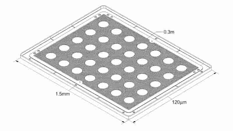
PCB stencils (also called SMT stencils) are precision-engineered stainless steel tools used to apply solder paste accurately onto printed circuit boards during surface mount technology assembly. They ensure consistent, high-quality solder paste deposition, critical for reliable electronic connections.
Key Benefits of Our High-Precision PCB and SMT Stencils
- Ultra-precise laser cutting for fine-pitch PCB components down to 01005 size
- Consistent solder paste release reducing assembly defects by up to 80%
- Long-lasting 304 stainless steel construction for extended service life
- Customizable thickness and aperture designs for specific PCB assembly needs
- Fast global delivery with 24-hour prototype turnaround
Types of SMT Stencils We Provide
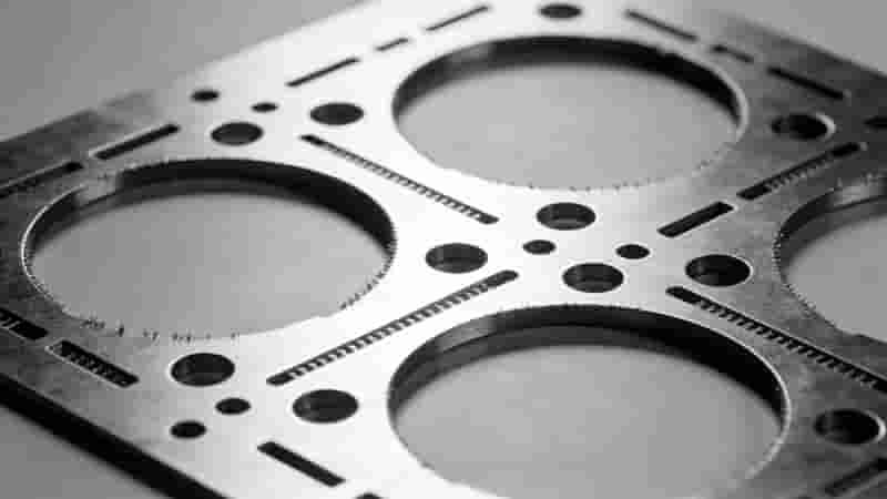
Laser-Cut SMT Stencils
Our most popular option, featuring high-precision laser cutting for clean apertures and excellent paste release. Ideal for standard to high-complexity PCB applications.
Framed SMT Stencils
Mounted on durable aluminum frames for automatic printing machines. Perfect for high-volume PCB production environments.
Frameless SMT Stencils
Cost-effective foil stencils compatible with universal frames. Great for prototyping and low-volume PCB assembly.
Nano-Coated SMT Stencils
Special nano-coating improves paste release for ultra-fine pitch components like BGAs and QFNs, essential for advanced PCB designs.
SMT Stencil Type Comparison
| Stencil Type | Best For | Precision Level | Delivery Time |
|---|---|---|---|
| Laser-Cut | General PCB Assembly | High | 24 Hours |
| Framed | High-Volume Production | Ultra-High | 24-48 Hours |
| Frameless | Prototyping & Small Runs | High | 24 Hours |
| Nano-Coated | Fine-Pitch PCB Components | Maximum | 48 Hours |
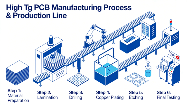
Our PCB and SMT Stencil Manufacturing Process
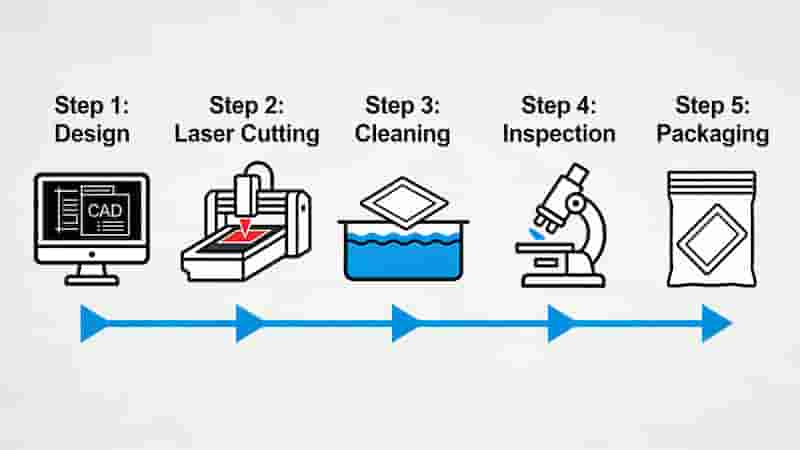
We follow a rigorous, standardized process to ensure every PCB stencil meets the highest industry standards:
- Design Verification: Comprehensive review of Gerber files and PCB specifications
- Material Preparation: Premium 304 stainless steel sheets selected for optimal performance
- Precision Cutting: Advanced laser cutting with 0.001″ beam accuracy
- Polishing & Finishing: Smooth aperture walls for perfect solder paste release
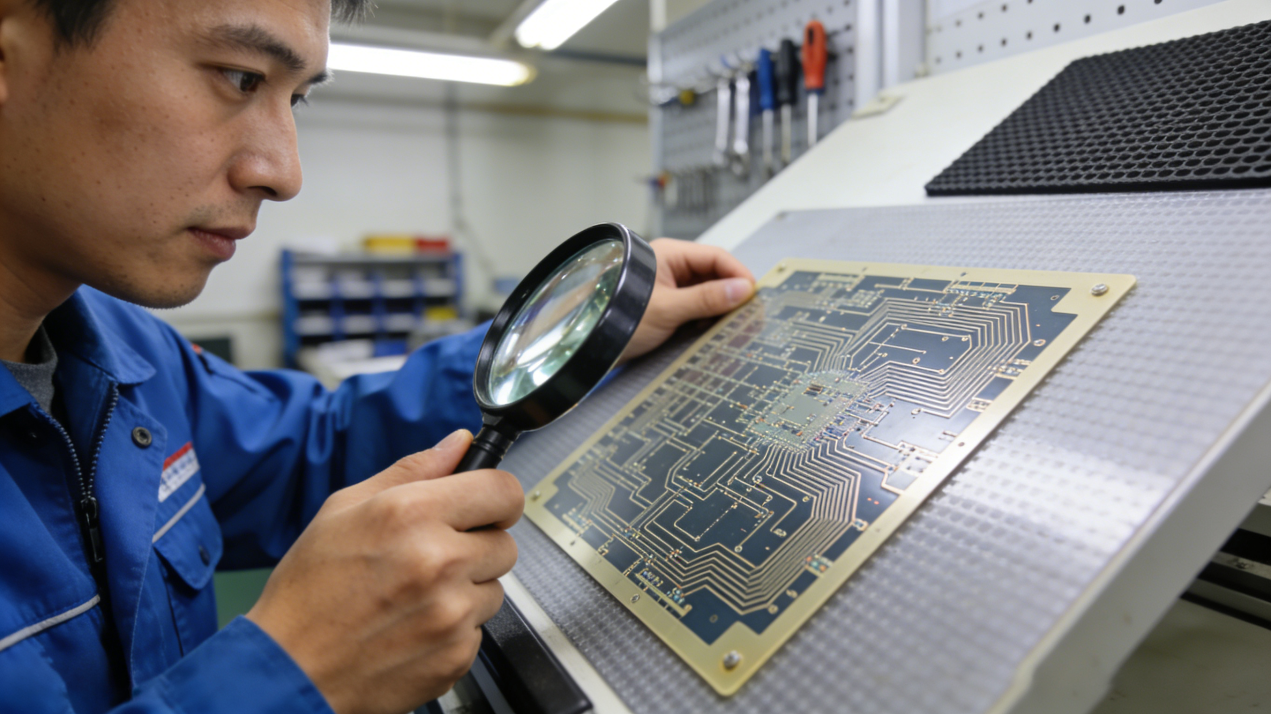
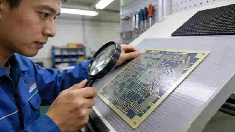
- Quality Inspection: 100% inspection under magnification to ensure precision
- Packaging & Shipping: Secure packaging to protect stencils during global delivery
Manufacturing Process Overview
| Step | Process | Key Activity | Quality Gate |
|---|---|---|---|
| 1 | Design Verification | Gerber file review, DFM analysis | Aperture design confirmation |
| 2 | Material Preparation | 304 stainless steel sheet selection | Material certification check |
| 3 | Precision Cutting | Laser cutting with 0.001″ accuracy | Dimensional verification |
| 4 | Polishing & Finishing | Aperture wall smoothing | Surface roughness inspection |
| 5 | Quality Inspection | 100% magnification review | Aperture quality approval |
| 6 | Packaging & Shipping | Secure packaging, global delivery | Final shipment verification |
Technical Specifications for PCB and SMT Stencils
- Material: SUS 304 Stainless Steel
- Thickness Range: 0.001″ – 0.007″ (0.025mm – 0.178mm)
- Minimum Aperture Size: 0.004″ (0.1mm)
- Cutting Precision: ±0.0005″ (0.0127mm)
- Frame Sizes: Customizable to match all standard printers
- Surface Treatment: Standard or nano-coating available
Quality Control and Industry Standards
All our high-precision PCB and SMT stencils are manufactured in compliance with:
- IPC-7525 Standard for Stencil Design
- ISO 9001 Quality Management System
- RoHS Directive Compliance
Each stencil undergoes rigorous testing including dimensional verification, aperture quality inspection, and solder paste release testing before shipment.
Summary
We specialize in high-precision PCB and SMT stencil manufacturing for global electronics manufacturers. Our custom stencils deliver exceptional precision, reliability, and consistency for all SMT assembly applications. With strict quality control, fast delivery, and expert technical support, we are your trusted partner for all PCB stencil needs.
Get Your Custom PCB and SMT Stencil Quote Today
Contact us for a free, no-obligation quote on your high-precision PCB stencil requirements. Our engineering team is ready to assist with your specific needs.
Request Free Quote