Key Differences Between Prototype and Production PCBs Explained

PCB Lead Time Comparison Prototype and Mass Production Volume

Understanding prototype PCBs and production PCBs is essential for engineers, buyers, and project managers. This guide breaks down critical differences in lead time, cost, design flexibility, materials, testing, quality standards, and manufacturing processes to help you make informed decisions for your electronics projects.

Introduction

Printed circuit boards are foundational to nearly all electronic devices. The journey from concept to mass production relies on two critical stages: prototype PCB development and full-scale production PCB manufacturing. Each stage serves a unique purpose, with distinct requirements for speed, cost, precision, and reliability.

Mastering the differences between these two phases helps reduce risks, shorten time-to-market, lower overall costs, and ensure final product performance and durability for global industrial and commercial applications.
Prototype PCB vs Production PCB Overview Design and Manufacturing

Lead Time & Order Volume

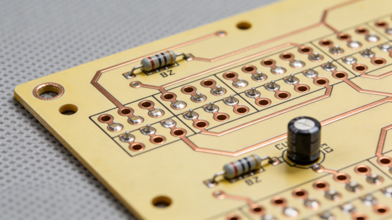
Prototype PCBs prioritize speed for rapid design validation. Typical order volumes are 5 to 50 pieces, with lead times as fast as 24 to 48 hours for urgent projects.

Production PCBs focus on high-volume consistency. Orders range from hundreds to tens of thousands of units, with standard lead times of 2 to 6 weeks due to tooling, process setup, and full quality validation.
PCB Lead Time Comparison Prototype and Mass Production Volume

Design Flexibility & Change Control

Prototype PCBs support frequent design iterations. Engineers can adjust layouts, components, and routing to optimize functionality without high rework costs.

Production PCBs require strict change control. Once tooling and production lines are set, modifications lead to significant delays, extra costs, and yield risks. A complete DFM (Design for Manufacturability) review is mandatory before mass production.

Quality Standards & Testing

Prototype PCBs focus on basic functional verification. Testing includes continuity checks and simple performance validation to confirm design feasibility.

Production PCBs follow strict industry standards such as IPC-A-600 and undergo comprehensive testing: solderability, thermal cycling, insulation resistance, signal integrity, and environmental stress screening to ensure long-term reliability.

Materials & Manufacturing Processes

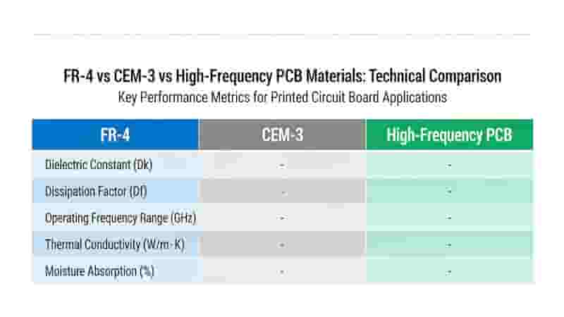
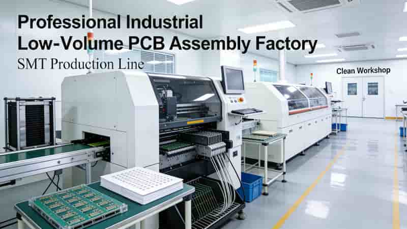
Prototype PCBs use standard materials like FR-4 and rapid fabrication methods such as laser direct imaging (LDI) to deliver fast turnaround.

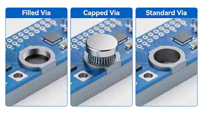
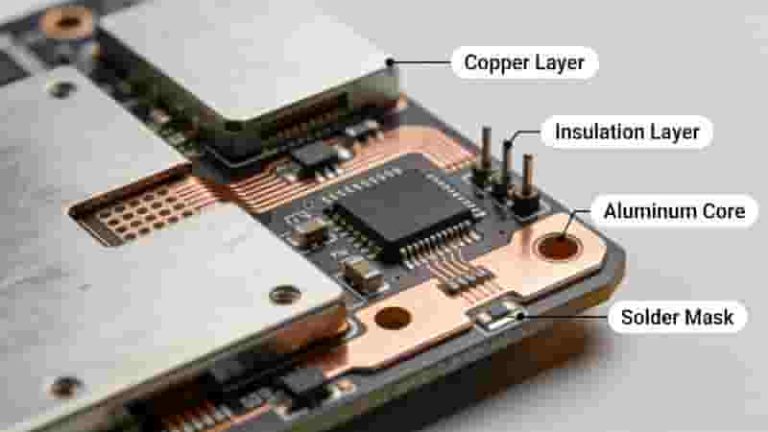
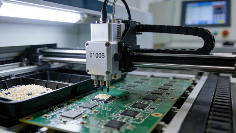
Production PCBs use high-performance materials including high-Tg FR-4, Rogers, and metal-core substrates. Advanced processes include HDI, impedance control, blind/buried vias, and automated manufacturing for precision and consistency.
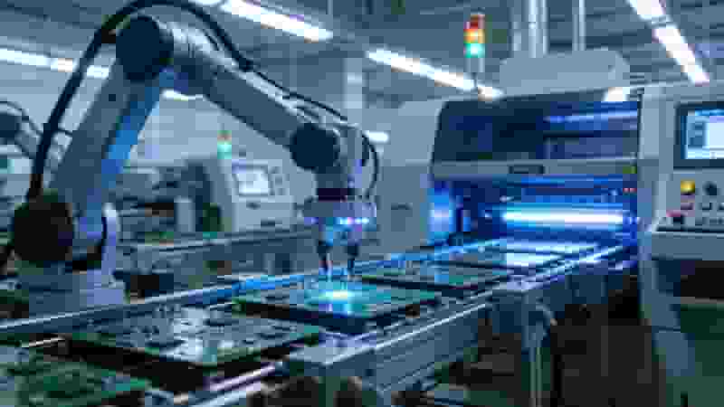
PCB Materials and Manufacturing Process Prototype vs Production

Cost Structure & Pricing

Prototype PCBs have a higher per-unit cost due to small-batch production, but total project cost is low for validation purposes.

Production PCBs benefit from economies of scale, resulting in much lower per-unit costs. One-time costs include tooling, stencils, and setup fees, which are amortized across large volumes.

Full Comparison Table: Prototype vs Production PCBs

AspectPrototype PCBsProduction PCBs
Lead Time24h – 7 days2 – 6 weeks
Order Volume5 – 50 pieces100 – 100,000+ pieces
Design ChangesFlexible, low costStrictly controlled, high cost
Testing LevelBasic functional checkFull IPC compliance & reliability test
MaterialsStandard FR-4High-grade & specialty substrates
Per-Unit CostHigherMuch lower (scale efficiency)

Conclusion & Key Takeaways

Choosing between prototype PCBs and production PCBs depends on your project stage, volume needs, timeline, and performance requirements.

Use prototype PCBs for design validation, testing, and small-batch verification. Switch to production PCBs when your design is finalized, stable, and ready for high-volume deployment with consistent quality and cost efficiency.
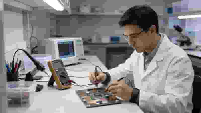
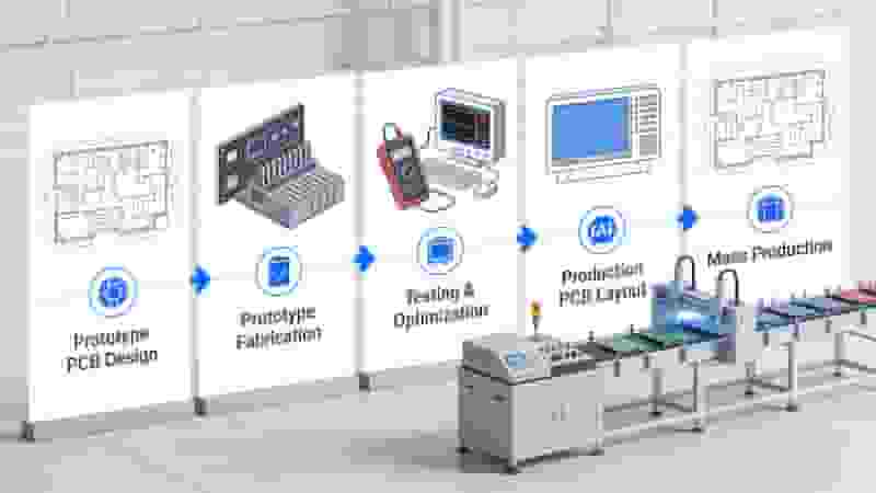
PCB Prototype to Production Transition Workflow for Engineers

Inquiry & Custom PCB Solutions

We provide reliable prototype PCB and production PCB manufacturing services for global buyers, engineers, and industrial clients. Get professional DFM review, fast lead times, competitive pricing, and full-quality assurance.

Contact us today for a free quote, custom solution, or technical support for your next PCB project.

Request a Free PCB Quote
Copper Core PCB Structure - High Thermal Conductivity Copper Base

Copper Core PCB vs. Metal Core PCB: Key Differences & Advantages

Posted on
0 Comments
Copper Core PCB delivers superior thermal conductivity and stability for high-power electronics, while Metal Core PCB offers cost-effective thermal management for general industrial and commercial applications. Introduction to PCB Technology Printed Circuit Boards (PCBs) are the foundational building blocks of modern electronic devices. From consumer electronics to industrial machinery, PCBs ensure reliable electrical connectivity and…
HASL PCB industrial applications industrial control LED automotive

HASL: Hot Air Solder Leveling for PCB Surface Finish
Posted on
0 Comments
HASL (Hot Air Solder Leveling) is a widely used, cost-effective PCB surface finish that protects copper pads from oxidation and ensures reliable solderability for industrial and commercial electronics assembly. What Is Hot Air Solder Leveling (HASL)? Hot Air Solder Leveling (HASL) is a mature and industry-standard PCB surface finish applied to exposed copper circuits. It…
Heavy Copper PCB thermal management and heat dissipation structure

Heavy Copper PCB Manufacturing & Thick Copper PCB Fabrication Service

Posted on
0 Comments
We provide custom heavy copper PCB and thick copper PCB solutions up to 12oz for high‑current, high‑thermal power electronics, automotive, industrial, and military applications. As a professional heavy copper PCB manufacturer, we deliver engineering‑driven fabrication with optimized stackups, reliable plating, and robust solder mask for long‑term performance under high current and harsh environments. Prototypes and…
Cross Section of Plated Half Hole PCB

Understanding Plated Half-Holes (Castellated Holes) in PCB Design

Posted on
0 Comments
Plated half-holes, also called castellated holes, provide a space-efficient way to interconnect separate PCB modules by soldering. Unlike bottom pads, their edge positioning simplifies mounting and enhances reliability. This article explains everything about plated half-hole structures, design guidelines, manufacture, benefits and use cases. Structure of Plated Half-Holes Plated half-holes, also known as castellated holes, resemble…
Advantages of OSP PCB surface finish for fine pitch SMT

PCB OSP Surface Finish: Complete Technical Guide for Buyers & Engineers

Posted on
0 Comments
OSP (Organic Solderability Preservative) is a lead‑free, RoHS‑compliant organic coating applied to exposed copper pads on printed circuit boards to prevent oxidation and preserve solderability before SMT assembly. This guide explains PCB OSP surface finish in full: process, pros, cons, storage, assembly, comparisons, and best practices for industrial electronics manufacturing. What Is PCB Surface Finish?…
Plated Through Hole PTH Structure in PCB

What is the Difference Between PTH and Via in PCBs?

Posted on
0 Comments
Understanding the key differences between PTH and via is essential for optimizing PCB design and manufacturing. This article defines PTH and via, compares dimensions, functions, locations and finishing requirements. Typical applications and design considerations are also discussed. Defining PTH and Vias in PCBs PCBs serve as the foundation for almost all modern electronics. They provide…

FAQs About Prototype PCB vs Mass Production PCB Distinction & Selection

A: Prototype 5~50pcs with 24h~7d fast delivery; mass production hundreds to tens of thousands, standard cycle 2~6 weeks for full setup and QC validation.

A: Prototype supports frequent low-cost layout modification; production locks tooling, any design change brings extra expense and long production delay.

A: Prototype only basic continuity & simple function test; production executes full IPC standard plus thermal cycling, insulation and environmental reliability screening.

A: Prototype mostly regular FR4 + LDI rapid process; mass production adopts high-Tg FR4/Rogers/MCPCB plus HDI, impedance, blind/buried via mature automated production.

A: Small batch cannot amortize setup/stencil expense; large volume shares fixed tooling cost to realize scale cost reduction.

A: R&D design verification period for function debugging, layout optimization and performance verification before finalizing design.

A: After design fully finalized, all prototype tests passed and no further layout modification needed for bulk market shipment.

A: Qualified integrated PCB factory supports seamless transition from small prototype to large-batch production without changing vendors.

Similar Posts