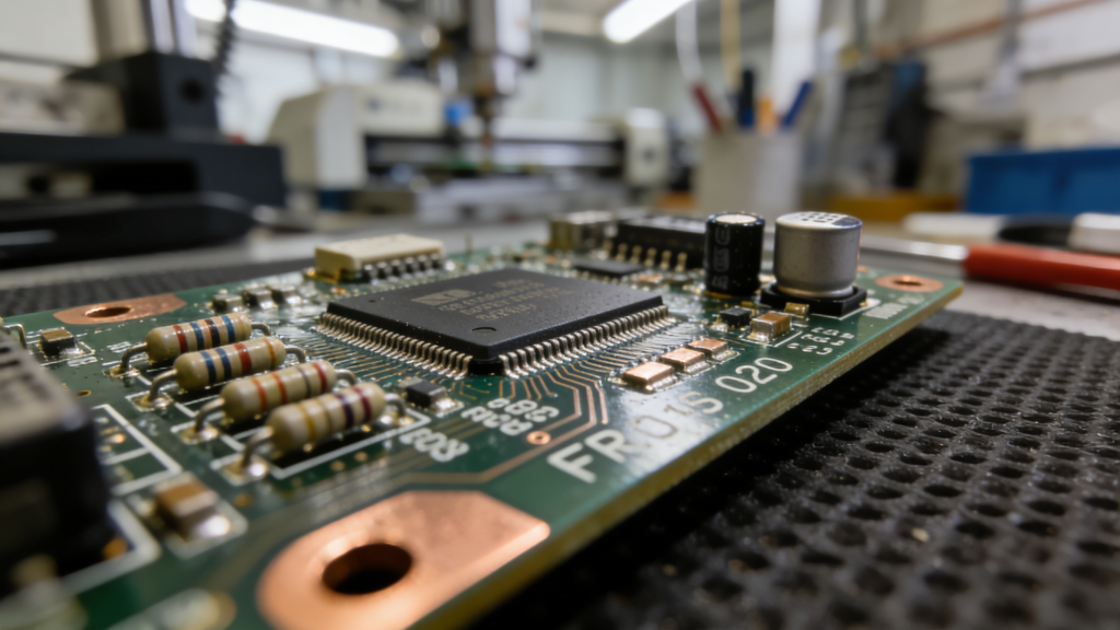
FR-4 is the most widely used flame-retardant glass-epoxy laminate material for rigid PCB manufacturing. Defined by NEMA standards, it offers excellent electrical insulation, mechanical strength, thermal stability, and cost efficiency, making it the global industry standard for most electronic applications.
What is FR-4 Material?
FR-4 (Flame Retardant Grade 4) is a NEMA-defined material grade for PCB substrates, not a specific material name. It indicates the resin self-extinguishes after combustion and meets the UL94 V-0 flammability standard.
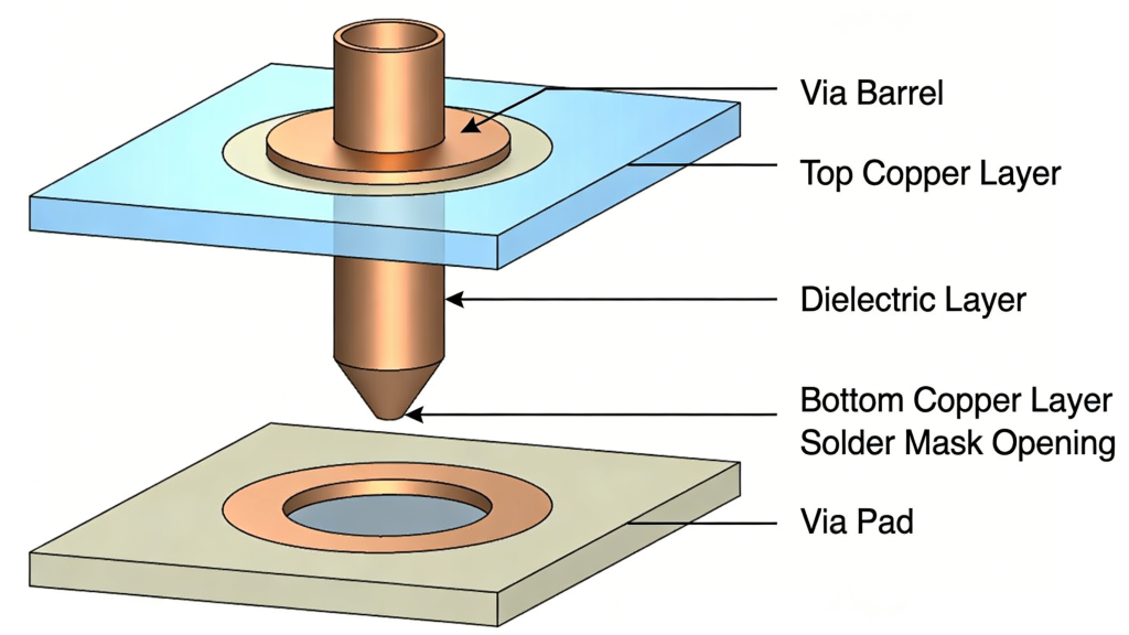
FR-4 uses brominated epoxy resin for fire resistance and electronic-grade woven fiberglass cloth as reinforcement. It is laminated with copper foil under high temperature and pressure to form Copper Clad Laminate (CCL), the core material for rigid printed circuit boards.
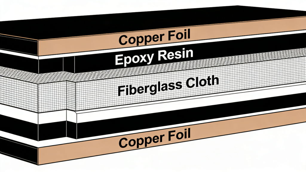
FR-4 Composition & Laminate Structure
A standard FR-4 laminate consists of three core components that determine its performance in PCB fabrication:
- Woven fiberglass cloth: Provides rigidity, tensile strength, and dimensional stability
- Flame-retardant epoxy resin: Delivers electrical insulation and self-extinguishing properties
- Copper foil: Forms conductive circuits on one or both sides of the laminate
This composite structure makes FR-4 ideal for single-sided, double-sided, and multilayer PCB production.
Key Technical Properties of FR-4
FR-4 offers balanced performance critical for reliable PCB operation across industries:
- Flammability: UL94 V-0 rated, self-extinguishing, no fire spread
- Glass Transition Temperature (Tg): Standard 130°C; high-Tg up to 180°C+
- Electrical insulation: High dielectric strength, low leakage current
- Dielectric constant (1MHz): ~4.4, stable for general circuits
- Mechanical strength: High flexural strength, resistant to warping
- Moisture absorption: Low rate, stable in humid environments
- Cost efficiency: Lower cost than high-frequency or special materials
FR-4 vs Other PCB Substrate Materials
| Material | Flame Retardant | Tg (°C) | Best For |
|---|---|---|---|
| FR-4 | UL94 V-0 | 130–180+ | Most rigid PCB |
| CEM-3 | UL94 V-0 | 120–130 | Low-cost double-sided PCB |
| FR-2 | UL94 V-1 | ~105 | Single-sided consumer PCB |
| High-Frequency | UL94 V-0 | 180–250 | RF/microwave circuits |
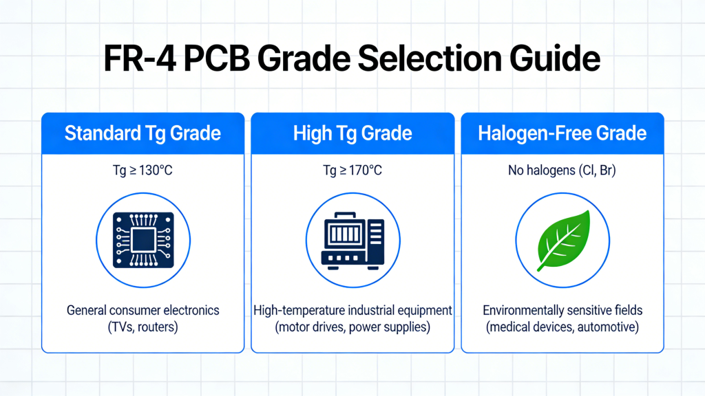
FR-4 Grades & Selection Guide
FR-4 substrates are classified by performance to match different PCB requirements:
- Standard Tg FR-4 (130°C): General-purpose consumer and industrial electronics
- Mid Tg FR-4 (150°C): Automotive and industrial control applications
- High Tg FR-4 (170–180°C+): Lead-free soldering, high-temperature environments
- Halogen-free FR-4: Eco-friendly, RoHS compliant for medical and automotive
- High CTI FR-4: High tracking resistance for industrial power devices
FR-4 Standard Parameters & Thickness
Common FR-4 specifications for PCB fabrication:
- Board thickness: 0.3mm, 0.4mm, 0.5mm, 0.6mm, 0.8mm, 1.0mm, 1.2mm, 1.5mm, 1.6mm, 2.0mm
- Copper weight: 0.5oz, 1oz (standard), 2oz (high current)
- Dielectric constant (Er): 4.2–4.7 @ 1MHz
- Dissipation factor (Df): ≤0.04 @ 1MHz
- CTI: ≥600V for high-performance grades
Typical FR-4 PCB Applications
FR-4 is the first choice for most PCB applications due to its versatility:
- Consumer electronics: smartphones, laptops, home appliances
- Industrial control: automation equipment, instruments, power supplies
- Automotive: infotainment, sensors, lighting, control units
- Communication: routers, base stations, network devices
- Medical: diagnostic equipment, monitoring devices
Conclusion
FR-4 is the global standard material for rigid PCB fabrication, offering unmatched balance of performance, reliability, and cost. It meets the requirements of most electronic applications from consumer products to industrial and automotive systems.
Choosing the right FR-4 grade (standard Tg, high Tg, halogen-free) ensures your PCB design performs reliably in its operating environment.
Ready for Your FR-4 PCB Project?
We provide professional FR-4 PCB manufacturing, custom prototyping, and mass production with fast lead times and strict quality control.
Get a Free Quote
Demystifying THT PCB Assembly: A Comprehensive Professional Guide
PCB Drilling Process: Full Technical Guide for Manufacturing & Quality
PCB Vias: Complete Guide to Types, Design, Reliability & Applications
Via-in-Pad for Printed Circuit Boards: Complete Technical Guide
What Is the Difference Between PTH and Via in PCBs?