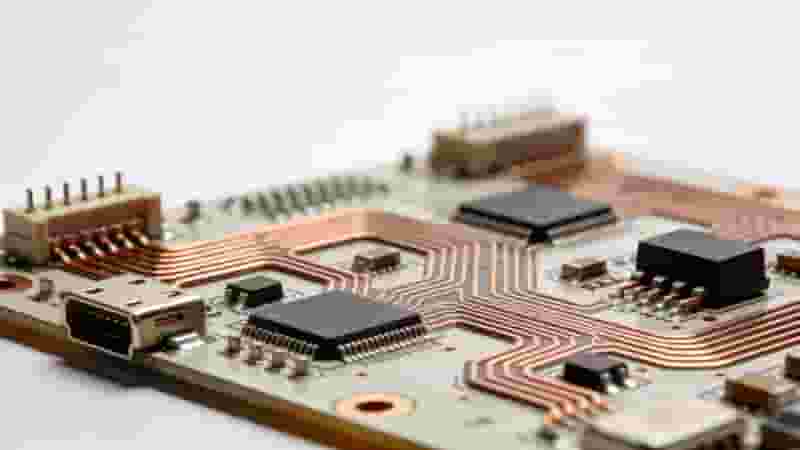
Via-in-Pad technology places vias directly within surface mount pads to save space, improve routing efficiency, and enhance PCB density for HDI and high-speed designs.
What Is Via-in-Pad Technology for PCBs?
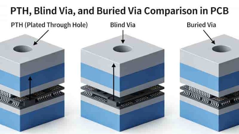
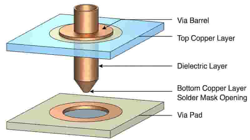
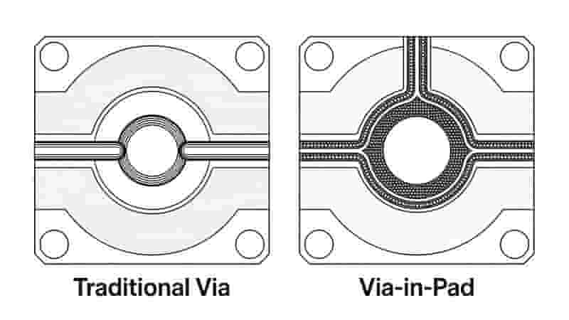
Before understanding via-in-pad, let’s review common PCB via types: Plated-through holes (PTHs) span the entire board, blind/buried vias connect partial layers, and microvias (~0.1mm) link adjacent layers. All serve layer-to-layer interconnection.
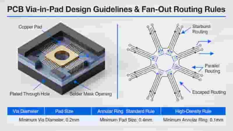
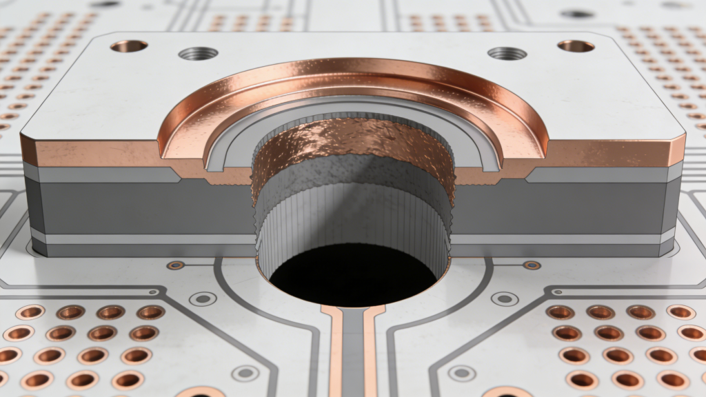
Via-in-pad is an advanced HDI PCB design that places vias directly inside surface mount pads. By merging pads and vias into one structure, it eliminates fanout traces and frees up routing space. IPC standards define various types, with space efficiency as the core advantage.
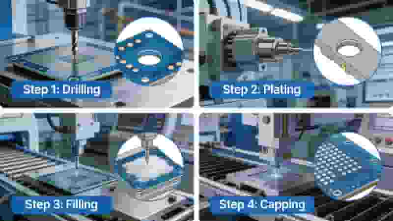
As an experienced PCB manufacturer, we specialize in reliable via-in-pad fabrication, including precision drilling, plating, tinning, and solder mask processing. We help customers achieve higher density, fewer layers, and simplified circuits.
Key Benefits of Via-in-Pad for PCBs
Via-in-pad significantly improves PCB efficiency by combining pad and via functions. The main advantages include:
- Higher component density: Reduces pad/via footprint by up to 50%, enabling smaller products or more features.
- Layer reduction: Complex designs can cut 2–4 layers, lowering material and production costs.
- Better routing: Increases channel space by up to 30%, shortening traces and reducing noise in analog circuits.
- Lower cost: Eliminates extra drilling steps and simplifies assembly, cutting total project expenses.
This makes via-in-pad ideal for wearables, IoT, automotive, and mobile electronics where miniaturization is critical.
Challenges of Via-in-Pad & Solutions
While via-in-pad offers great benefits, designers must address these challenges for long-term reliability:
- Solder wicking: Use proper solder mask and filled/capped vias to prevent solder leakage.
- Reflow heat balance: Adjust thermal profiles to compensate for higher pad/via thermal mass.
- Rework difficulty: Plan layouts carefully since rework on via-in-pad is limited.
- Drilling precision: Maintain ±0.1mm accuracy to ensure valid annular rings.
- Thermal stress: Follow DFM rules to reduce material expansion mismatch risks.
We provide full-process validation, including thermal shock testing and X-ray inspection, to ensure robust via-in-pad performance.
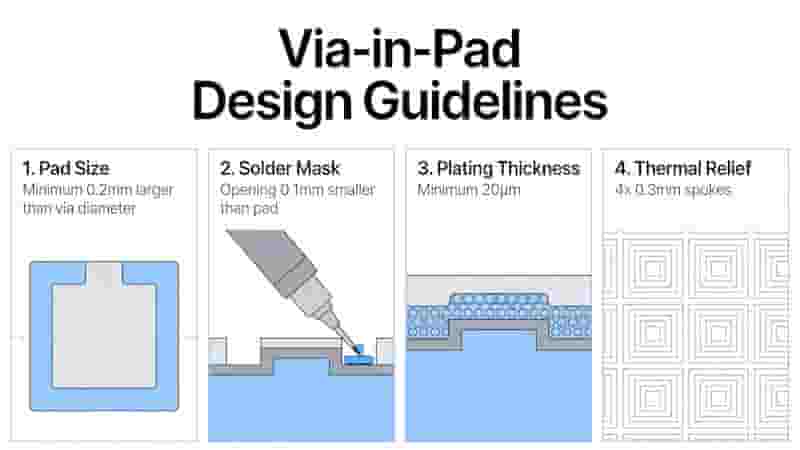
Via-in-Pad Design Guidelines (IPC Compliant)
Follow these industry-proven rules to optimize via-in-pad performance and manufacturability:
- Solder mask: Open 0.2–0.3mm larger than via diameter for isolation.
- Surface finish: Immersion silver or nickel performs better against solder leaching.
- Dimensions: 0.15mm vias for 0201 components; 0.3–0.5mm for BGA pads.
- Tenting: Tented vias reduce wicking but restrict rework.
- Thermal relief: Use copper spokes to dissipate reflow heat evenly.
- Testing: Validate with thermal cycling, shear testing, and microsectioning.
We offer professional DFM support to refine your via-in-pad designs before production.
Reliability & IPC Standards for Via-in-Pad
Via-in-pad reliability is validated under IPC-6012D, the global standard for rigid PCBs. Key tests include:
- Thermal cycling: 100 cycles from -55°C to 125°C with no cracks or failures.
- Mechanical shock: 1500G loads across 3 axes to verify structural integrity.
- Liquid exposure: Test insulation under moisture and chemical conditions.
- Microsectioning: Inspect plating quality and void levels.
- X-ray inspection: Confirm drill alignment, annular rings, and bonding.
We follow these strict standards to deliver durable, high-quality via-in-pad PCBs for industrial, medical, and automotive use.
Best Applications for Via-in-Pad PCBs
Via-in-pad delivers the most value in these scenarios:
- Ultra-compact designs: Wearables, smartphones, and compact IoT devices.
- Cost-sensitive projects: Reduces layer count and total cost.
- High-SMT boards: Fine-pitch BGAs, QFNs, and 0201 components.
- High-speed/analog circuits: Shorter traces improve signal integrity.
High-power or high-mechanical-stress designs may still use traditional vias based on application needs.
Summary & Custom PCB Inquiry
Via-in-pad is a foundational HDI technology that boosts PCB density, reduces layers, improves routing, and cuts costs. With proper design and manufacturing, it offers excellent reliability for modern electronics.
We are a professional PCB manufacturer specializing in via-in-pad, HDI, multilayer, and high-speed PCBs. We provide full support from DFM to mass production.
Contact us today for a free quote, design review, or custom via-in-pad PCB solution tailored to your project!
Impedance Control PCB Fabrication Services
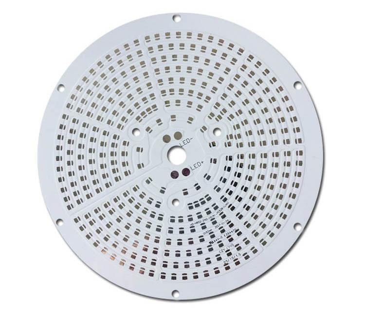
Aluminum PCB Manufacturing Process: Step-by-Step Guide
Understanding Plated Half-Holes (Castellated Holes) in PCB Design
PCB Vias: Complete Guide to Types, Design, Reliability and Performance
Why Choose FR-4 as Your PCB Material in 2025? The Definitive Guide