Blind Vias & Buried Vias in PCBs – The Complete Technical Guide
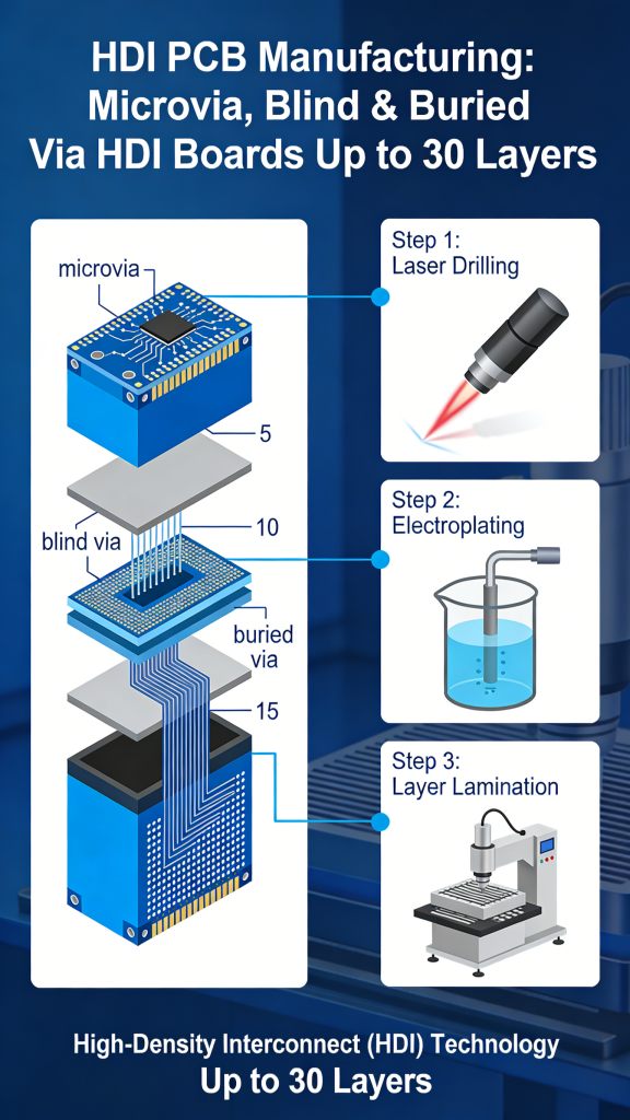
Blind vias and buried vias enable superior signal routing, component density, electrical performance, and simplified stackups for complex high‑speed designs. This guide defines both via types, explains key differences, design rules, manufacturing, applications, and implementation best practices for engineers and buyers.
Introduction
As printed circuit boards grow more complex and highly integrated, advanced via structures meet demanding routing and layering needs. Traditional plated‑through holes (PTHs) have inherent limits, pushing designers to adopt blind vias and buried vias in multilayer boards.
These vias optimize performance, density, and cost for high‑speed, high‑density interconnect (HDI PCB) applications. Understanding their differences supports better design and manufacturing decisions for reliable, cost‑effective boards.
What Are Blind Vias?
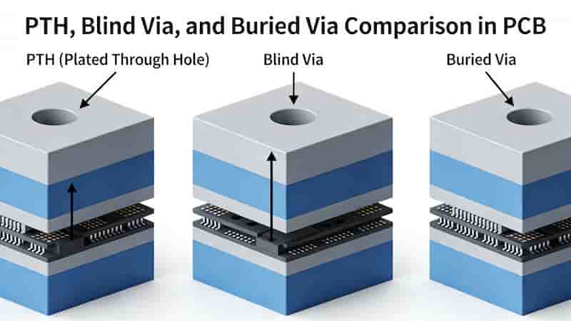
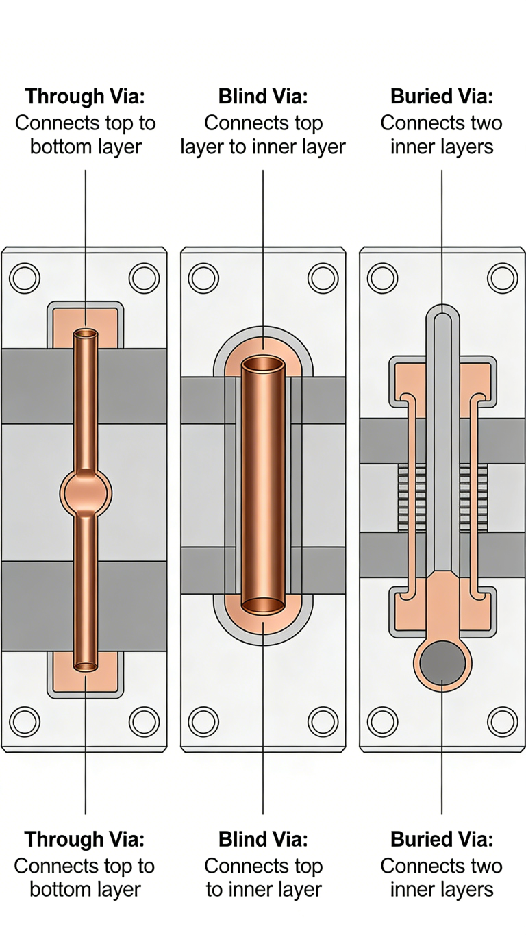
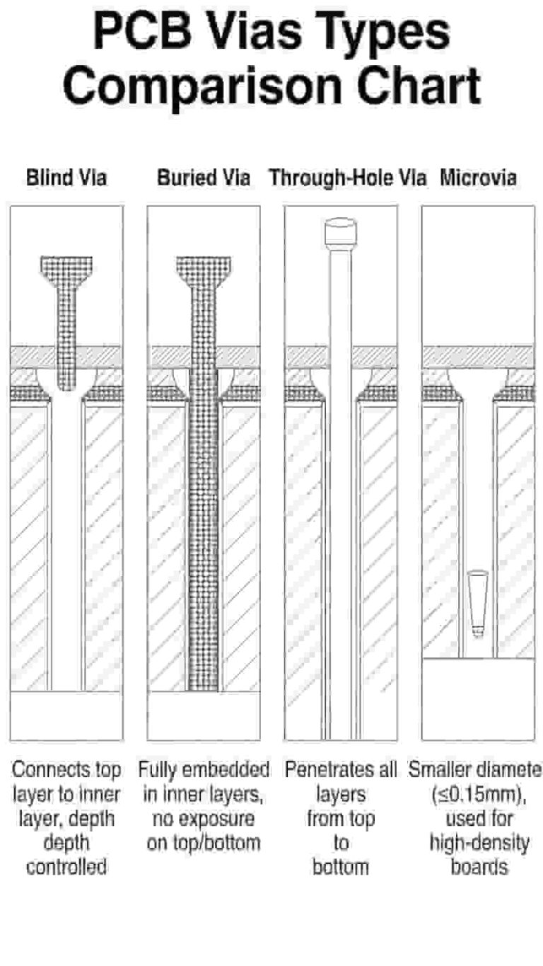
A blind via forms an electrical connection between one outer layer and one or more inner layers without fully penetrating the PCB stackup. It terminates internally and remains visible only from one external surface.
Key Characteristics:
Connects one external layer to internal layers
Does not pass through the full board thickness
Leaves the opposite outer layer intact
Common in boards of 6 layers or more
Smaller diameter than standard PTH vias
Requires high‑precision drilling and alignment
Core Benefits:
Higher component density: saves surface space by ~15–20%
Flexible routing for dense, complex layouts
Lower material and lamination cost vs. full PTH designs
What Are Buried Vias?
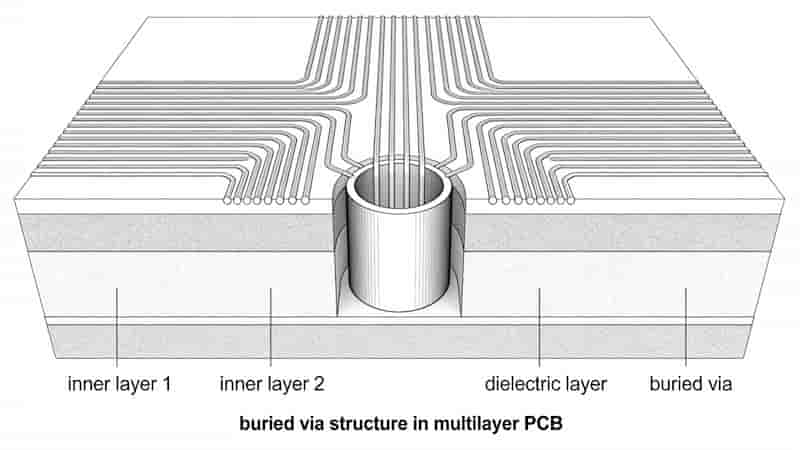
A buried via connects two or more internal layers only, with no exposure to either outer surface. It is fully embedded inside the PCB and invisible after lamination.
Key Characteristics:
Connects inner layers only; no outer‑layer contact
Requires tight layer registration
Ideal for high‑density interconnects
Not accessible for visual or physical inspection
Core Benefits:
Reduces total layer count and simplifies stackups
Improves signal integrity with short, direct paths
Lower parasitic capacitance for high‑frequency performance
Shields inner signals from outer‑layer interference
Key Differences Between Blind Vias and Buried Vias
Parameter
Blind Vias
Buried Vias
Connectivity
Outer → inner layers
Inner → inner layers only
Penetration
Partial stackup penetration
Embedded; no outer exposure
Inspection
One‑sided visual/probe access
No visual or probe access
Manufacturing
Controlled‑depth drilling
Sequential lamination
Best Use Case
Space‑saving HDI PCBs
High‑speed, high‑layer‑count boards
Design & Manufacturing Considerations
Successful use of blind vias and buried vias requires strict adherence to fabrication capabilities and reliability rules.
Manufacturing Capabilities
Verify manufacturer supports target layer counts and via sizes
Registration tolerance ≤ ±0.002” for high precision
Extra lamination, drilling, and plating steps affect cost and lead time
Testing & Inspection
Buried vias need X‑ray or advanced microscopy
Impedance, continuity, and resistance testing are mandatory
Blind vias allow partial visual and probe inspection
Reliability & Design Rules
Account for thermal stress and moisture expansion risks
Follow manufacturer annular ring, spacing, and size guidelines
Limit high‑via‑count designs to 6–8 layers to control yield
Industry Applications
Blind vias and buried vias are foundational to modern HDI PCB and high‑speed electronics:
High Density Interconnect (HDI) PCBs: Boost routing density by >20% vs. standard multilayer boards
High‑Speed Digital Circuits: Improve signal integrity for SERDES, high‑data‑rate links
RF & High‑Frequency Designs: Reduce parasitics and stabilize impedance
Automotive Electronics: Support miniaturization and high integration
Portable & Wearable Devices: Enable compact form factors without performance loss
Conclusion
Blind vias and buried vias are essential for advanced PCB design, delivering higher density, better signal performance, and optimized stackups compared to traditional PTH vias. Blind vias link outer and inner layers for space efficiency; buried vias connect inner layers for high‑speed reliability.
Success depends on aligning design rules with manufacturing capabilities. With careful planning, these vias solve miniaturization, speed, and density challenges for industrial, automotive, consumer, and telecom products.
Need Custom PCBs with Blind Vias & Buried Vias?
We specialize in reliable HDI and multilayer PCB manufacturing with advanced blind and buried via processing. Get a free DFM check, fast quotation, and tailored production for your global project.
FR-4 is the global industry-standard flame-retardant glass-reinforced epoxy laminate for rigid PCB fabrication. This guide explains definition, composition, properties, grades, selection, and why FR-4 PCB is the top choice for engineers and global buyers. What is FR-4 Material? FR-4 (Flame Retardant Type 4) is a NEMA-defined material grade for flame-resistant epoxy laminates. It is not…
FR-4 is the global industry-standard flame-retardant glass-reinforced epoxy laminate for rigid printed circuit boards. Defined by NEMA LI-1 and IPC-4101, it delivers balanced electrical insulation, mechanical strength, thermal stability, UL94 V-0 flame resistance, and cost efficiency for industrial, automotive, telecom, and consumer electronics. What is FR-4 Material? FR-4 (Flame Retardant Type 4) is a material…
A Surface Mount Device (SMD) component package is a standardized enclosure designed for direct soldering onto PCB surfaces, enabling high-density assembly, miniaturization, and automated manufacturing in modern electronics. What Is an SMD Component Package? SMD stands for Surface Mount Device, referring to electronic components designed exclusively for Surface Mount Technology (SMT) assembly. An SMD component…
We provide end-to-end turnkey PCB assembly supporting full and partial models, with SMT assembly, THT, BGA/QFN, rigorous testing, and global logistics for industrial buyers, engineers, and importers. What Is Turnkey PCB Assembly Turnkey PCB assembly is a one-stop manufacturing solution covering PCB fabrication, component sourcing, assembly, testing, and delivery. We manage the full supply chain…
We provide reliable through-hole PCBAs assembly service for industrial, power, medical, aerospace and automotive applications. Our IPC-standard THT assembly supports prototypes to mass production with wave soldering, selective soldering and full inspection. Through-hole PCB Assembly Service Overview Our through-hole PCB assembly fulfills leaded assembly demands across industries. We deliver single-sided, double-sided and high-density multilayer through-hole…
Standard PCB thickness is critical for mechanical strength, signal integrity, and assembly compatibility. This guide covers definitions, industry standards, influencing factors, manufacturing constraints, and design best practices for global industrial buyers. What Is Standard PCB Thickness The global standard PCB thickness is 1.57 mm (0.062 in), commonly referenced as 1.6 mm for simplicity. This is…
We provide professional SMT PCB assembly services supporting rapid prototypes to high-volume production. Certified to IPC‑A‑610 Class 2/3, ISO 9001, RoHS, we deliver precision assembly for 01005 components, fine‑pitch BGAs, rigid/flex/rigid‑flex PCBs with full inspection and global delivery. Core SMT PCB Assembly Capabilities We support full‑process SMT PCB assembly from prototype validation to stable mass…
We provide professional single layer PCB manufacturing and cost-effective single sided PCBs for LED lighting, power supplies, consumer electronics, and industrial equipment. Our ISO & IPC‑certified production ensures stable quality, fast lead times, and free DFM analysis for prototypes and mass production. Single-Layer PCB Definition A single layer PCB (also called single sided PCB) has…
We are a leading China-based Rigid-Flex PCB manufacturer specializing in 1–12 layer rigid-flex PCB prototype, small-to-large volume fabrication, and full assembly with fast turnaround, free DFM check, and ISO/UL/RoHS certification. Benefits of Rigid-Flex PCB Rigid-Flex PCB integrates the stability of rigid boards with the flexibility of flex circuits, delivering superior performance for compact, high‑reliability electronic…
Get reliable quick turn PCB assembly with one-stop PCB fabrication, components sourcing, SMT/THT assembly and testing, helping you turn ideas into working boards in days instead of weeks. What Is Quick Turn PCB Assembly Service? Quick turn PCB assembly is an accelerated manufacturing process that integrates PCB fabrication, component sourcing, SMT/THT assembly and testing to…
PCB Solder Mask (also known as solder resist) is a protective polymer layer applied to printed circuit boards to prevent solder bridging, resist oxidation, improve insulation, and ensure long‑term reliability in SMT assembly and industrial applications. This guide covers definitions, types, colors, processes, DFM rules, IPC standards, testing, and troubleshooting for engineering and procurement teams…
We provide high-quality, low-cost PCB prototypes and professional PCB assembly for global engineers and buyers. Reliable, fast, and cost-effective PCB solutions from 2-layer to multilayer, flexible, and rigid-flex boards. Why Choose Us for Low-Cost PCB Prototypes We balance affordable PCB prototypes with consistent, industrial-grade quality. Our advantages help you reduce costs while ensuring reliability: Factors…
We offer professional multilayer PCB manufacturing services in China supporting 4 to 30 layer rigid, flex, and rigid-flex PCBs. Our high-reliability boards serve industrial, telecom, medical, aerospace, and automotive applications with ISO 9001, IATF 16949, IPC-A-610 Class 3, UL, and RoHS compliance. Multilayer PCB Manufacturing Capabilities We provide comprehensive multilayer PCB manufacturing with precise specifications…
FR-4 is the most widely used flame-retardant glass-epoxy laminate material for rigid PCB manufacturing. Defined by NEMA standards, it offers excellent electrical insulation, mechanical strength, thermal stability, and cost efficiency, making it the global industry standard for most electronic applications. What is FR-4 Material? FR-4 (Flame Retardant Grade 4) is a NEMA-defined material grade for…
HDI PCB manufacturing provides high-density interconnect solutions with microvia, blind via, and buried via structures for compact, high-performance electronics. We deliver reliable HDI boards from prototype to mass production, supporting up to 30 layers for automotive, 5G, medical, and industrial applications. What Is HDI PCB and Why Choose It High-density interconnect (HDI) PCBs offer much…
We provide professional BGA PCB manufacturing, precision assembly, advanced rework, and full testing for high-reliability electronics. Our ISO/IPC-certified processes support prototypes to mass production for global industrial buyers, engineers, and procurement teams. What Is BGA (Ball Grid Array) and Why It Matters for Your PCB? A ball grid array (BGA) is a high-density surface-mount package…
Standard PCB thickness is typically 1.57 mm (0.062 inches), often rounded to 1.6 mm. This guide covers definitions, influencing factors, manufacturing constraints, non-standard design rules, and selection tips for industrial buyers and engineers. Quick Overview: standard PCB thickness (1.6mm) is industry default; common alternatives include 0.78mm (0.031in) and 2.36mm (0.093in). Thickness impacts durability, weight, assembly,…
We are a trusted Aluminum PCB manufacturer and MCPCB supplier in China, delivering fast prototypes and small‑to‑medium volume production for LED lighting, power supplies, and high‑power electronics. Our in‑house lines ensure stable quality, controlled costs, and on‑time delivery for global buyers. Aluminum PCB Manufacturing Capabilities With 15+ years of expertise in Aluminum PCB and MCPCB…
Looking for a trusted PCB manufacturer in South Africa for prototypes, mass production, or full PCBA? We deliver high-quality, cost-effective PCB manufacturing and assembly solutions to industrial buyers, engineers, and procurement teams across South Africa. Local PCB Manufacturing in South Africa We are a professional local PCB manufacturer serving South Africa with flexible lead times…
This professional guide covers PCB DFMA principles, IPC standards, manufacturability rules, assembly optimization, yield improvement, cost reduction, and global industrial best practices for reliable PCB and PCBA production. What is DFMA for PCB? DFMA (Design for Manufacturability and Assemblability) integrates DFM and DFA into a unified engineering framework to optimize PCB design for production efficiency,…
Flying Probe Testing for PCB is a fixtureless electrical testing method widely used for prototype, low-volume and high-mix printed circuit board production. It accurately detects opens, shorts, wrong components, reverse polarity and soldering defects without expensive custom fixtures, making it the top choice for engineering verification and small-batch manufacturing. What is Flying Probe Testing? Flying…
This guide details all essential PCB & PCBA manufacturing files, including Gerber files, BOM lists, NC Drill files, Centroid files, and other critical documents. It provides professional standards, format requirements, and technical parameters to ensure accurate quotes, error-free production, and reliable PCB assembly for global industrial buyers, engineers, and procurement teams. Core Files for PCB…
This guide covers everything about PCB solder mask (solder resist), including its functions, types, colors, application processes, thickness standards, IPC testing, and assembly compatibility. Learn how solder mask protects circuits, prevents solder bridging, and improves reliability for industrial and high-density PCBs. We explain how to select the right solder resist for rigid, flexible, and high-speed…
We specialize in LED PCB manufacturing and assembly with aluminum, copper & flexible substrates featuring superior heat dissipation. ISO 9001 certified, fast turnaround & competitive pricing for global LED lighting projects. Superior Heat Dissipation 1-9 W/mK thermal conductivity Fast Turnaround 24-hour quote, 3-5 days delivery ISO 9001 Certified International quality standard One-Stop PCBA Service From…
We deliver reliable SMT PCB Assembly for rapid prototypes, NPI, low-volume and high-volume production. Our full turnkey solutions support fine-pitch components, BGAs, QFNs, rigid/flex‑rigid PCBs, and comply with IPC Class 2 & Class 3 standards for global industrial buyers. SMT PCB Assembly Capabilities We support full‑cycle SMT PCB Assembly from single prototypes to mass production,…
We provide reliable through-hole PCBAs assembly service for industrial, power, medical, aerospace and automotive applications. Our IPC-standard THT assembly supports prototypes to mass production with wave soldering, selective soldering and full inspection. Through-hole PCB Assembly Service Overview Our through-hole PCB assembly fulfills leaded assembly demands across industries. We deliver single-sided, double-sided and high-density multilayer through-hole…
We provide professional single layer PCB manufacturing and cost-effective single sided PCBs for LED lighting, power supplies, consumer electronics, and industrial equipment. Our ISO & IPC‑certified production ensures stable quality, fast lead times, and free DFM analysis for prototypes and mass production. Single-Layer PCB Definition A single layer PCB (also called single sided PCB) has…
PCB Solder Mask (also known as solder resist) is a protective polymer layer applied to printed circuit boards to prevent solder bridging, resist oxidation, improve insulation, and ensure long‑term reliability in SMT assembly and industrial applications. This guide covers definitions, types, colors, processes, DFM rules, IPC standards, testing, and troubleshooting for engineering and procurement teams…
We provide professional Double Sided PCB manufacturer in China for global industrial buyers, engineers, and procurement teams. Our full capabilities cover prototyping, mass production, DFM, assembly, and strict quality control to meet IPC standards for reliable, high-performance double-layer PCBs. Why Choose Us for Double Sided PCB Manufacturing We are a professional manufacturer focused on Double…
Get a clear quote within 24 hours and receive high-quality PCB prototypes in as fast as 3-5 days, with one-to-one engineering support from inquiry to delivery. Get a Free Quote Now 24h quotation · 3-5 day PCB prototyping · One-stop PCB & PCBA Why Engineers and Buyers Choose Us From fast PCB prototypes to full…
FAQs About Blind Vias and Buried Vias
A: Blind vias connect outer layers to inner layers without penetrating the whole board. Buried vias link only internal layers and are fully hidden inside the PCB.
A: Blind vias are partially exposed for inspection, while buried vias are completely embedded. They apply different drilling and lamination processes for distinct connection needs.
A: They save board space, increase component density by 15-20%, enable flexible routing and cut down lamination costs for HDI layouts.
A: Buried vias shorten signal paths, lower parasitic capacitance, enhance signal integrity and protect inner circuits from external interference.
A: They are widely used in HDI PCBs, high-speed circuits, RF devices, automotive electronics and compact wearable products.
A: Blind vias support visual and probe inspection. Buried vias require X-ray or microscopic testing for internal quality check.
A: Yes. Extra drilling, sequential lamination and strict precision requirements raise production costs and extend lead time.
A: Follow requirements on via size, annular ring and spacing. Control layer quantity and account for thermal stress to guarantee production yield.
PCB vias connect layers in multilayer circuit boards, enabling compact, high-performance electronics. This guide covers plated through holes, blind, and buried vias, their design, manufacturing, and advantages in modern PCB fabrication. From 5G devices to automotive systems, understand how to choose the right via type for your project. PCB vias are the unsung heroes of…
Summary: This professional guide covers PCB vias definitions, core types, structure, design rules, aspect ratio, annular ring, manufacturing processes, and reliability standards. It helps engineers and buyers select the right via solutions for multilayer, high-speed, and HDI PCBs to ensure signal integrity, yield, and cost efficiency. What Are PCB Vias A via is a vertical…
This guide covers core PCB pad design principles, component spacing, IPC standards, SMD/through-hole rules, thermal management, and DFM to boost assembly yield, reliability, and performance for industrial and export-grade PCBs. PCB Component Layout & Spacing Rules When laying out PCB components, designers must balance minimum component spacing against component height and thickness. Proper spacing prevents…
Use professional PCB DFM analysis software to eliminate manufacturing risks, lower prototype costs, and speed up mass production for global electronics projects. What is PCB DFM Software PCB Design and PCB Manufacturing are two separate but closely linked systems. Design data cannot be directly used for production; it requires conversion to CAM (Computer-Aided Manufacturing) data….
A full professional overview of PCB vias including definitions, functions, types, manufacturing, reliability factors and advanced technologies for high‑performance multilayer printed circuit boards. Introduction: Definition, Role, and Types of Vias in PCBs A via is a vertical electrical connection between layers in a printed circuit board. Vias enable traces to transition between layers to facilitate…
PCB vias are essential vertical interconnects that enable layer transitions in multilayer printed circuit boards. This professional guide covers via definitions, core types, manufacturing processes, reliability factors, advanced structures, and best practices for engineers and global buyers. What Are PCB Vias A PCB via is a plated vertical electrical connection that routes signals, power, and…