Flying Probe Testing for PCB is a fixtureless electrical testing method widely used for prototype, low-volume and high-mix printed circuit board production. It accurately detects opens, shorts, wrong components, reverse polarity and soldering defects without expensive custom fixtures, making it the top choice for engineering verification and small-batch manufacturing.
What is Flying Probe Testing?
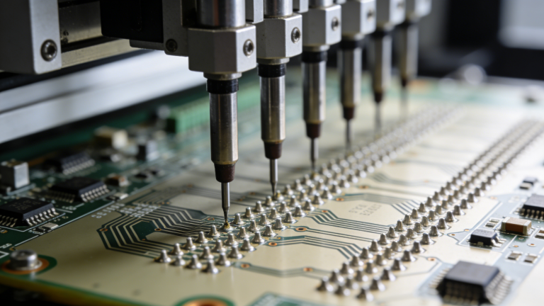
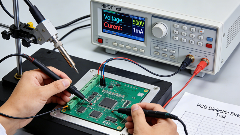
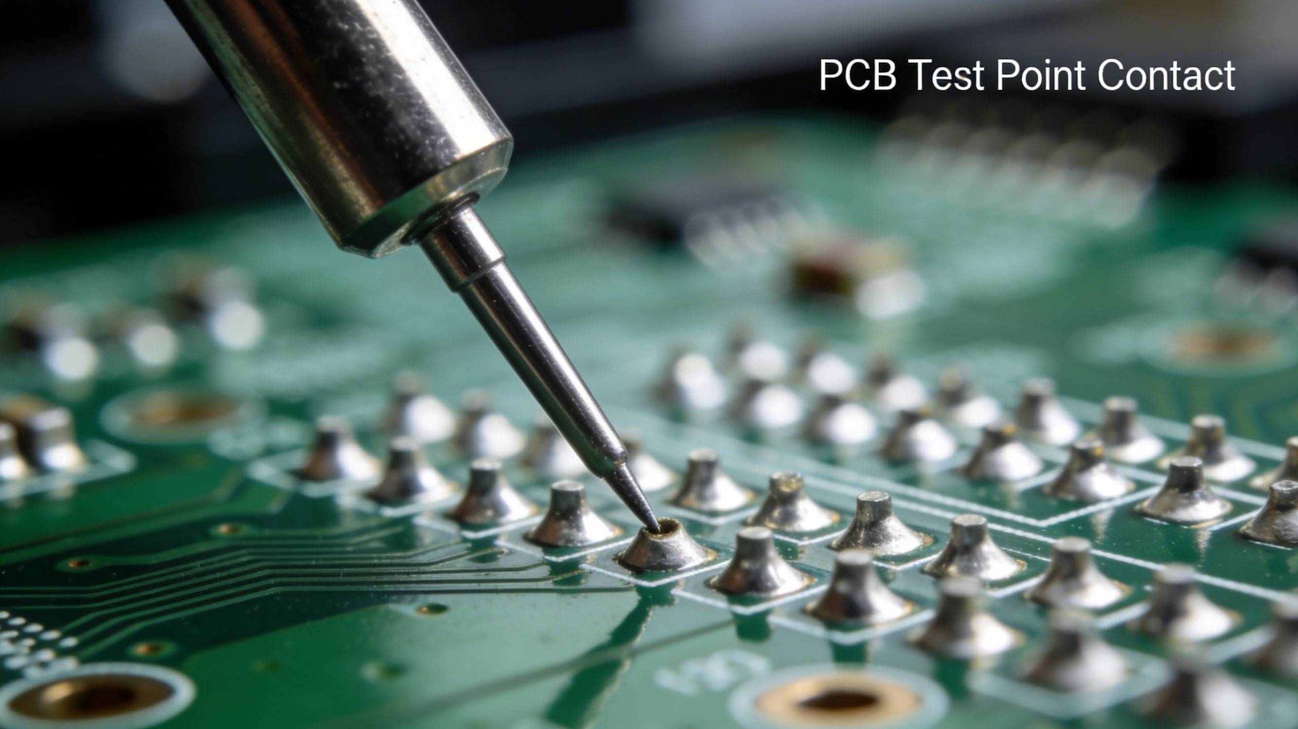
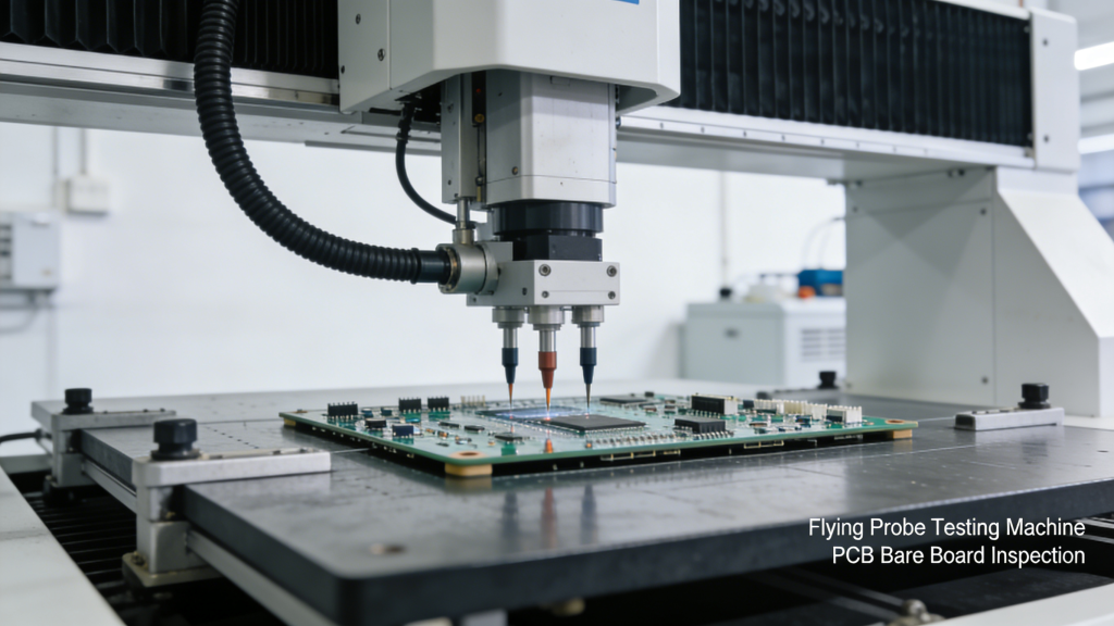
Flying Probe Testing for PCB is an automated electrical test method that uses movable probes to contact test points one by one to verify circuit integrity and component functionality. Unlike traditional bed-of-nails testers, it requires no custom fixture, which greatly reduces upfront cost and lead time.
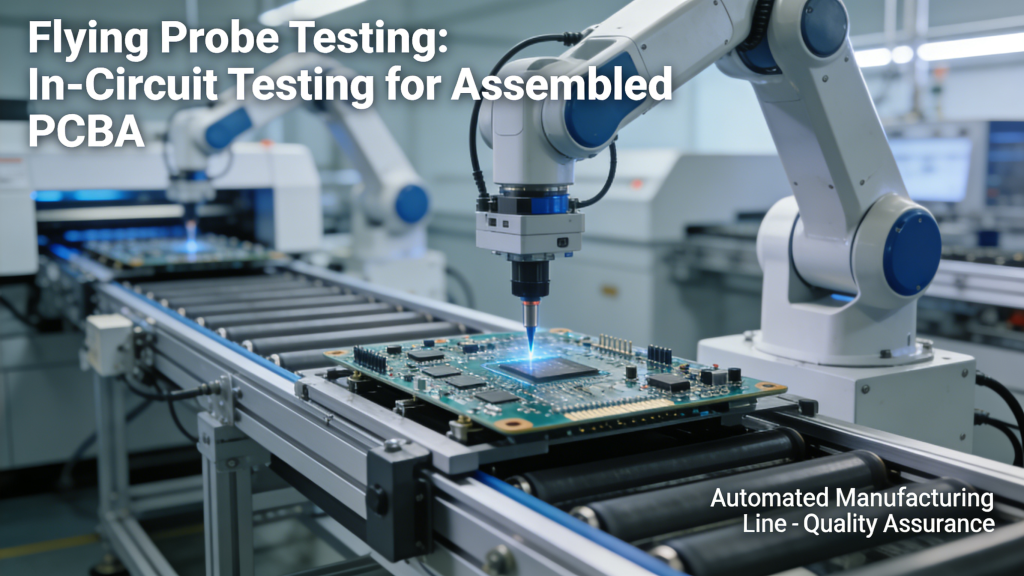
Modern flying probe systems support both bare PCB and assembled PCBA testing, covering electrical opens, shorts, wrong components, reversed polarity, missing parts and poor solder joints.
How Does Flying Probe Testing Work?
The process begins with importing Gerber, BOM and centroid files to generate a test program. The system then moves precision probes to target pads and test points automatically.
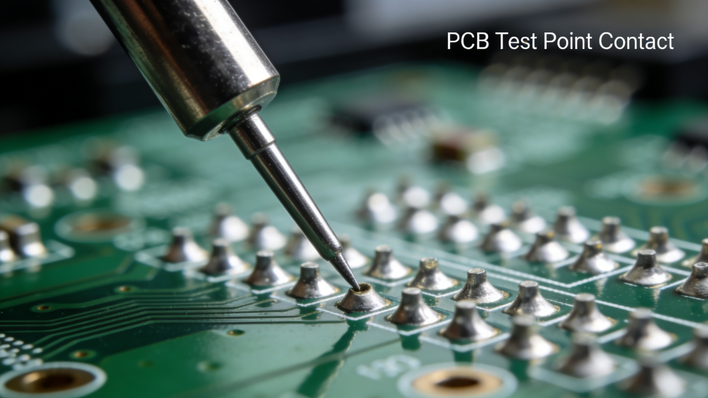
The tester applies low-voltage signals, measures resistance, capacitance and diode voltage, then compares real-time data with standard parameters to judge pass or failure. Defective boards are marked with precise fault locations for repair analysis.
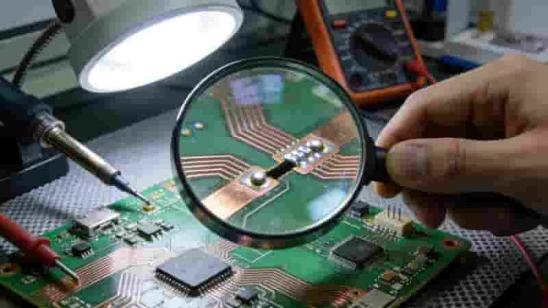
For assembled boards, flying probe testing for PCB also verifies component values, orientation and solder quality, ensuring full functional compliance before mass production.
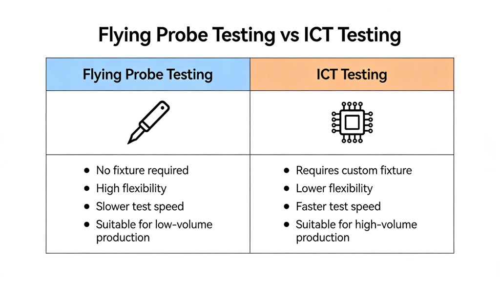
Flying Probe vs ICT Testing
| Item | Flying Probe Testing for PCB | ICT (Bed of Nails) |
|---|---|---|
| Fixture Required | No | Yes (High Cost) |
| Lead Time | Fast (Hours/Days) | Slow (Weeks) |
| Best For | Prototypes & Low Volume | High Volume Production |
| Test Speed | Medium | Very Fast |
| Upfront Cost | Low | High |
Advantages of Flying Probe Testing
- No expensive fixture, ideal for flying probe testing for PCB prototypes
- Short setup time, supports rapid engineering iterations
- High accuracy for opens, shorts and component defects
- Supports high-density boards (HDI) with small pads
- Flexible program editing for design changes
- Compatible with bare boards and assembled PCBA
Limitations
Although flying probe testing for PCB is powerful, it is less efficient for mass production because probes test points sequentially. For high-volume orders, ICT or functional testing is more cost-effective.
It also cannot perform simultaneous multi-point functional testing compared to dedicated fixture-based systems.
Ideal Applications
Flying Probe Testing for PCB is widely used in:
- PCB prototypes and R&D samples
- Low-volume & high-mix production
- High-density interconnect (HDI) boards
- Pre-mass production verification
- Reverse engineering and failure analysis
Conclusion
Flying Probe Testing for PCB remains the most practical and cost-efficient solution for prototype, small-batch and high-mix PCB manufacturing. It eliminates fixture cost, speeds up validation and ensures high reliability without compromising quality.
For projects requiring speed, flexibility and zero fixture investment, flying probe testing is the industry standard choice.
Need Professional Flying Probe Testing for Your PCB?
We provide reliable, fast and cost-effective flying probe testing for PCB and PCBA. Get a free quote and DFM analysis today.
Request a Quote
Through-hole PCB Assembly Service | IPC Certified THT PCBA Solutions
Multilayer Flexible PCB Manufacturer | Custom 4–16 Layer Flex Circuits
PCB Classification Guide: Types, Applications & Selection for Industrial Buyers
What is FR-4 Material in PCB Fabrication? The Complete Professional Guide
Low-Cost PCB Assembly Service | Reliable Provider & Cheap PCB Solutions