This professional guide covers PCB DFMA principles, IPC standards, manufacturability rules, assembly optimization, yield improvement, cost reduction, and global industrial best practices for reliable PCB and PCBA production.
What is DFMA for PCB?
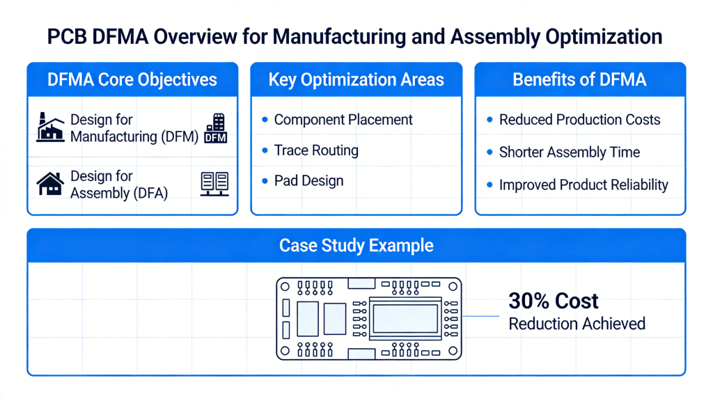
DFMA (Design for Manufacturability and Assemblability) integrates DFM and DFA into a unified engineering framework to optimize PCB design for production efficiency, cost control, quality stability, and fast assembly.
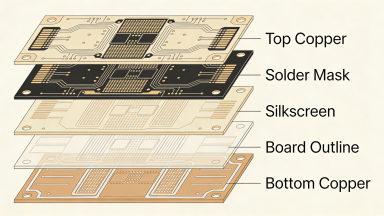
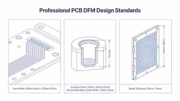
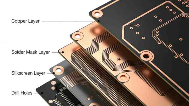
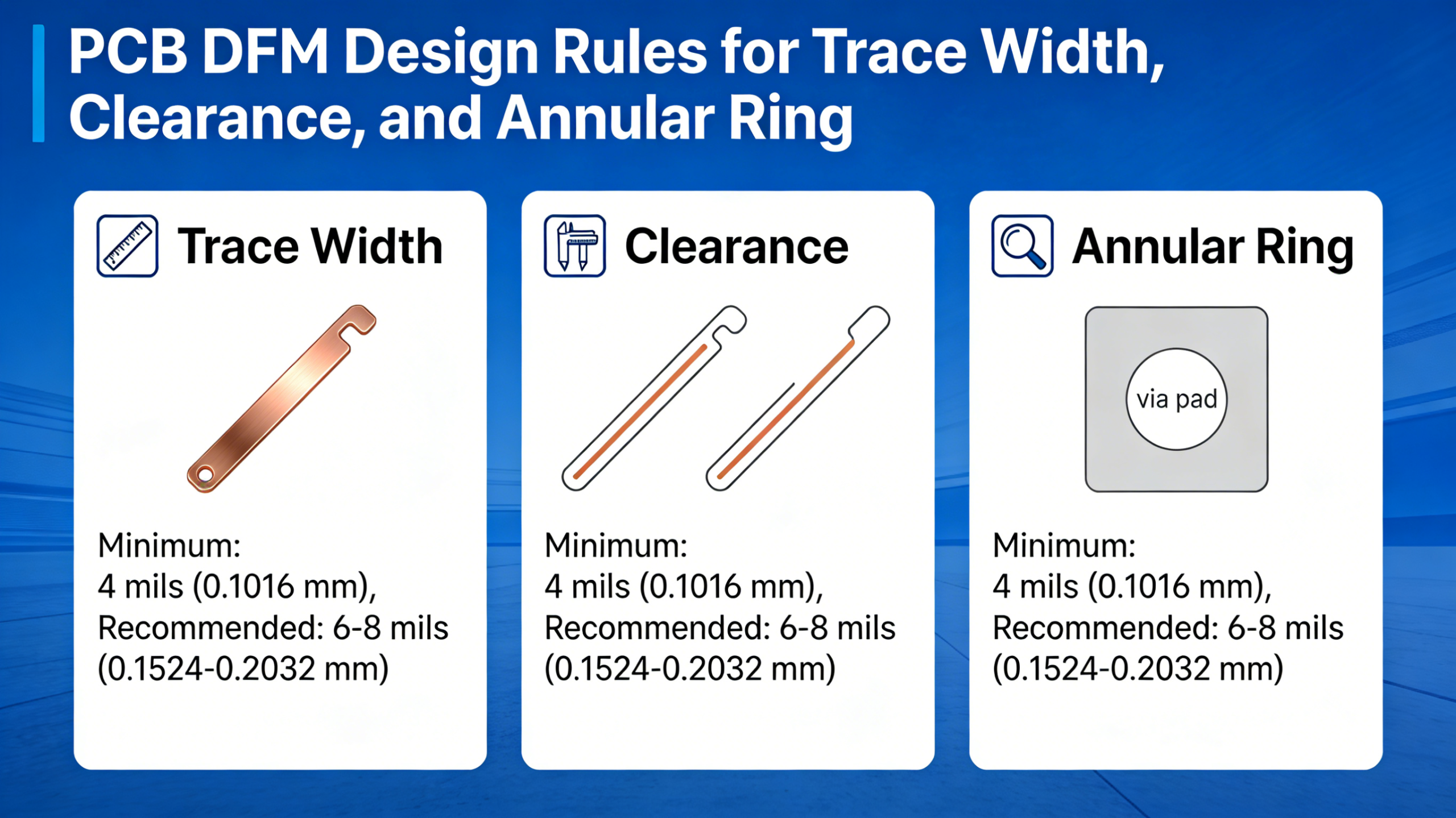
Design for Manufacturing (DFM) focuses on optimizing bare board fabrication: layer stackup, trace width, spacing, annular rings, hole size, solder mask, and material selection.
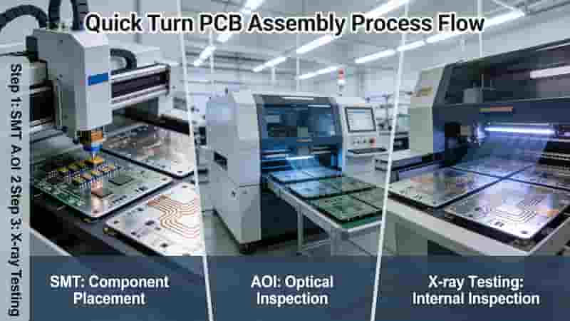
Design for Assembly (DFA) optimizes component placement, pad design, clearance, polarity, test points, and assembly process to minimize defects and speed up SMT and through‑hole assembly.
Core DFM Principles for PCB
DFM ensures your PCB design matches real manufacturing capabilities to avoid rework, delays, and high costs.
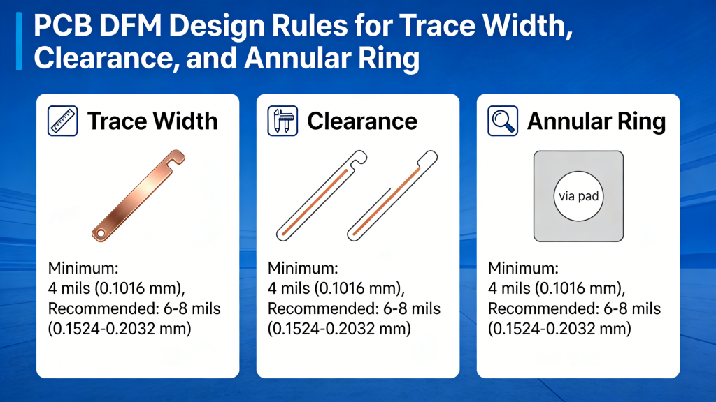
- Follow minimum trace and space per layer count and material
- Maintain valid annular ring for PTH and VIP holes
- Use standard hole sizes and avoid non‑standard drilling
- Ensure sufficient clearance from trace to board edge
- Optimize solder mask coverage and relief
- Standardize panelization and tooling features
- Comply with IPC‑2221 generic performance standard
Core DFA Principles for PCBA
DFA eliminates assembly risks and improves PCBA first‑pass yield.
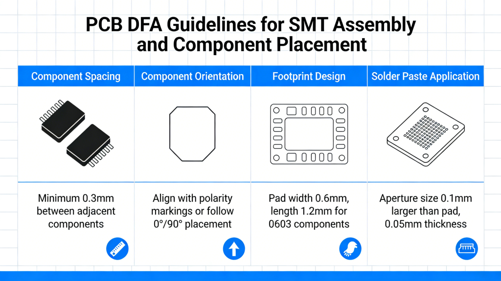
- Standardize component orientation and polarity marking
- Provide sufficient clearance between adjacent components
- Place test points for ICT and functional test
- Avoid small components near large connectors or heatsinks
- Use symmetrical design for balanced reflow soldering
- Label clear pin 1 and polarity indicators
PCB Manufacturability Analysis
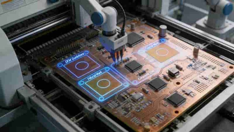
Manufacturability analysis uses rule‑based checking to validate PCB design against production capabilities early in the design phase.
Key analysis areas:
- Layer count and material compatibility
- Conductor spacing and impedance control
- Drill capability and aspect ratio
- Pad size and solderability
- Courtyard and component placement
- Panel design and assembly constraints
Automated DFM software reduces analysis time from days to hours and ensures consistency with IPC standards.
Benefits of DFMA Implementation
| Aspect | Without DFMA | With DFMA |
|---|---|---|
| Production Yield | Medium to Low | High & Stable |
| Lead Time | Long, with delays | Short & Predictable |
| Total Cost | Higher due to rework | Optimized & Lower |
| Quality Reliability | Variable | Consistently High |
- Reduce design iterations and engineering changes
- Lower material, labor, and scrap costs
- Improve PCB and PCBA reliability
- Speed up time‑to‑market for new products
- Support scalable mass production
IPC Standards for DFMA
Key industry standards for PCB DFMA:
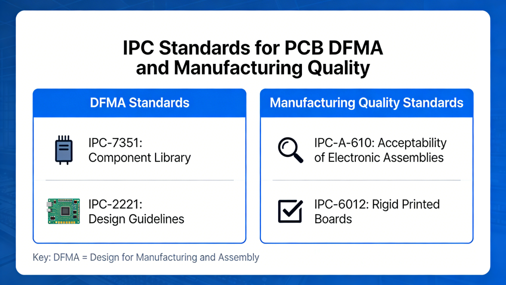
- IPC‑2221: Generic Standard for Printed Board Design
- IPC‑4101: Laminate Specifications
- IPC‑D‑300G: Printed Board Design Standard
- IPC‑A‑600: Acceptability of Printed Boards
- IPC‑7351: Land Pattern Standards
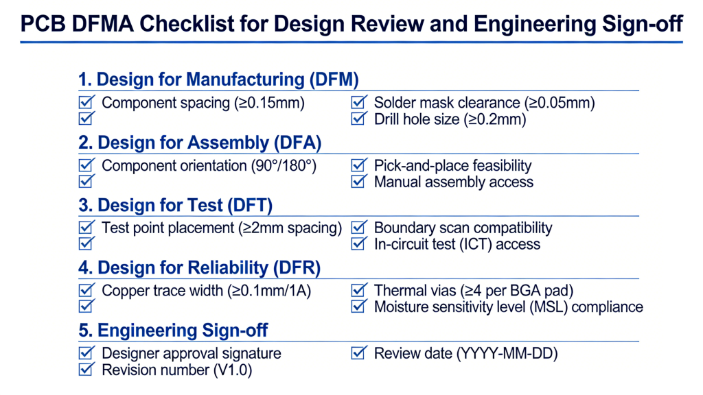
DFMA Checklist & Free Resources
A complete DFMA checklist ensures no critical design rule is missed.
- Trace width / space per layer and current
- Hole size and aspect ratio validation
- Pad and land pattern compliance
- Component clearance and height check
- Test point coverage
- Panelization and assembly feasibility
We provide a free downloadable DFMA checklist for your design team.
Conclusion
DFMA is essential for reliable, cost‑effective, and scalable PCB and PCBA manufacturing. By integrating DFM and DFA early in design, you achieve higher yield, lower cost, faster delivery, and stronger product performance for global markets.
Ready for Professional DFMA PCB Service?
Get free DFM analysis, fast quoting, custom engineering support, and high‑quality PCB & PCBA production.
Request DFMA Review & Quote
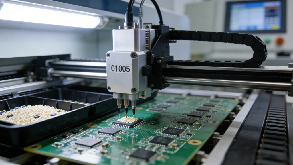
Turnkey PCB Assembly Services | Full & Partial Solutions
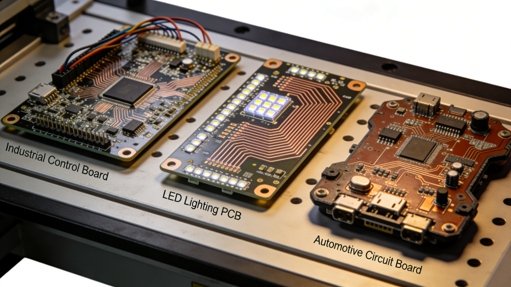
HASL: Hot Air Solder Leveling for PCB Surface Finish
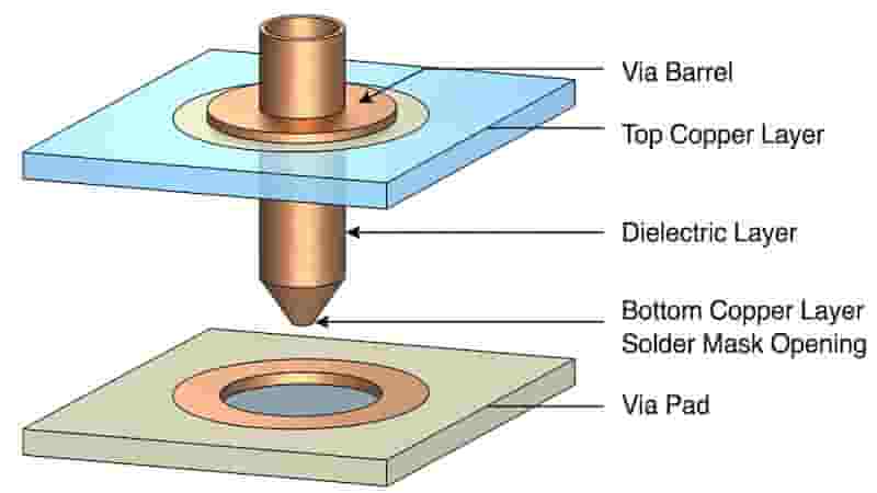
Via-in-Pad for Printed Circuit Boards: Complete Technical Guide

Turnkey PCB Manufacturing and Assembly: Full One-Stop Solution Advantages
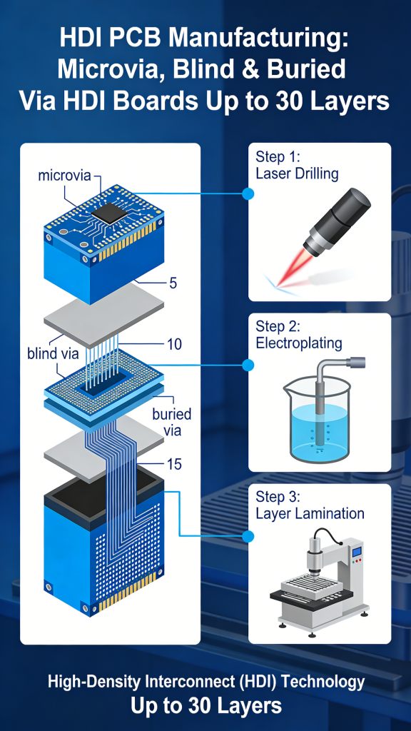
HDI PCB Manufacturing – Microvia, Blind & Buried Via HDI Boards up to 30 Layers