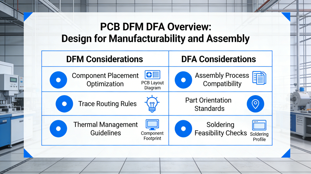
Optimize your PCB design for high yield, low cost, and reliable assembly with industry-leading DFM and DFA principles aligned with IPC standards.
What is Design for Manufacturing
Design for Manufacturing, also known as concurrent or simultaneous engineering, focuses on the relationship between product physical design and manufacturing systems. By integrating DFM principles into product design, the entire manufacturing process is optimized for efficiency and cost-effectiveness.
DFM reduces development cycles, lowers product costs, and accelerates time-to-market. It improves product quality, enhances manufacturability, shortens production time, and boosts overall work efficiency.
Beyond design specifications, DFM is a cross-departmental system activity that integrates processes, standards, and technologies. It considers functional requirements alongside lifecycle factors including manufacturability, efficiency, and economy.
DFM ensures designs meet optimal manufacturing conditions while supporting all external production requirements.
Free DFM PCB Design Checking
We provide free professional PCB design for manufacturability inspection services. Upload your PCB files today for a comprehensive review.
The Significance of Design for Manufacturing
- Reduces costs and enhances product competitiveness
- Enables production standardization and automation
- Facilitates technology transfer and inter-company collaboration
- Serves as the foundation for new product development and testing
- Addresses challenges in advanced electronic assembly techniques
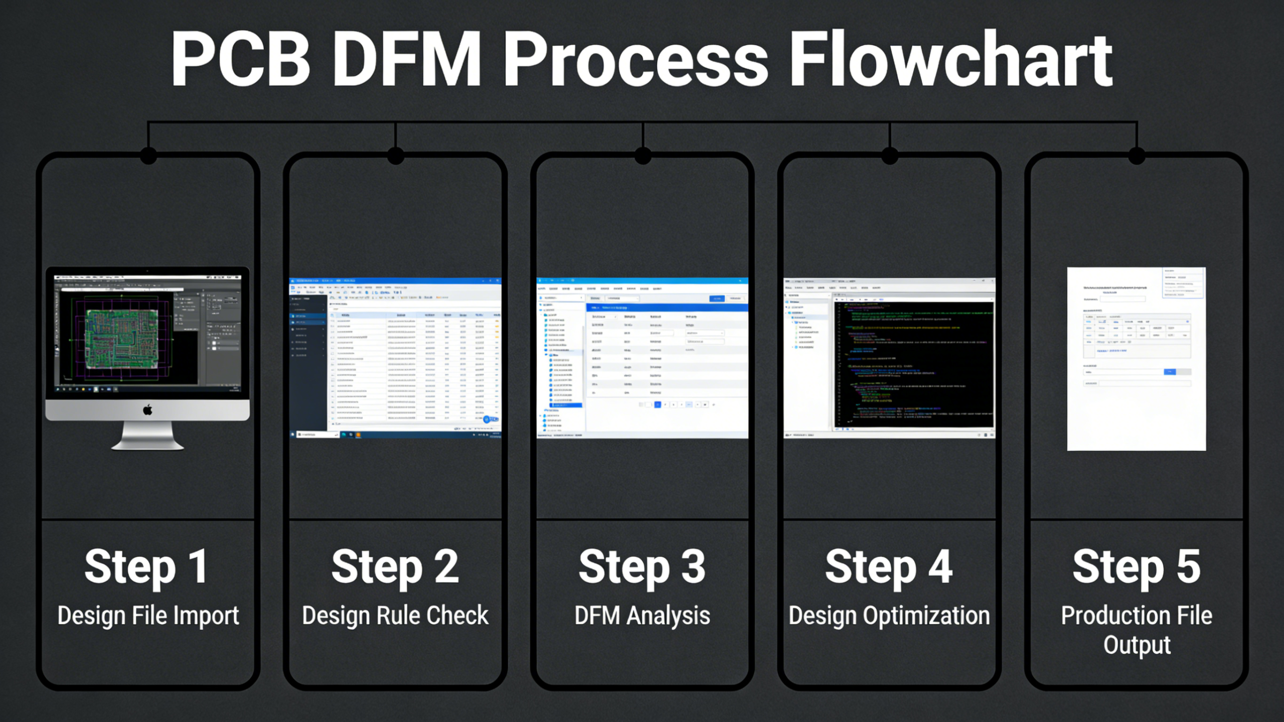
Process and Method of Design for Manufacturing
- Develop DFM specification documents
- Create DFM checklists during product design planning
- Generate comprehensive DFM reports
- Perform DFM testing and validation
- Conduct DFM analysis and evaluation
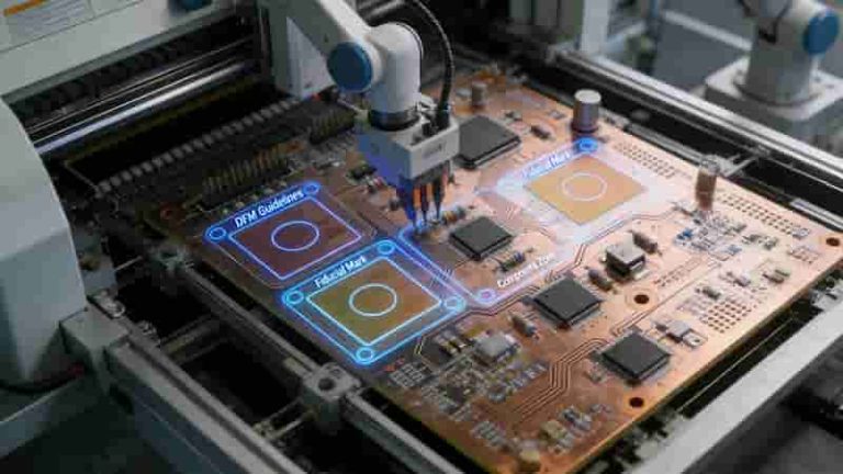
II. Manufacturability Analysis
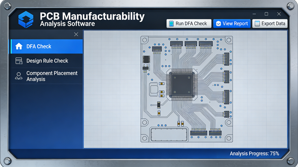
Manufacturability analysis, also called manufacturability review technology, allows designers to evaluate product producibility during the design phase. Using specialized tools and knowledge bases, designers refine designs to ensure they meet manufacturing requirements while maintaining functionality and quality.
DFM analysis manually assesses product efficiency, costs, and manufacturability.
2.1 Software Selection Indicators for Manufacturability Analysis
Effective DFM software should meet these technical criteria:
- Comprehensive inspection rule coverage
- User-friendly interface and learning curve
- Reliable operational stability
- Responsive customer support
- High-quality service provision
- Strict data confidentiality compliance
- Support for Excel and text BOM data
- CAD and BOM data verification capabilities
- PCB bare board manufacturability analysis
- Quick component library creation tools
- Component and rule library authority management
- Customizable inspection rules
- Excel and PDF report generation
- Custom development support
Without dedicated software, teams can create DFM checklists based on company specifications. These checklists systematically analyze product designs including:
- Product documentation such as schematics, PCB layouts, and assembly drawings
- Manufacturing process selection including AI, SMT, wave soldering, manual assembly
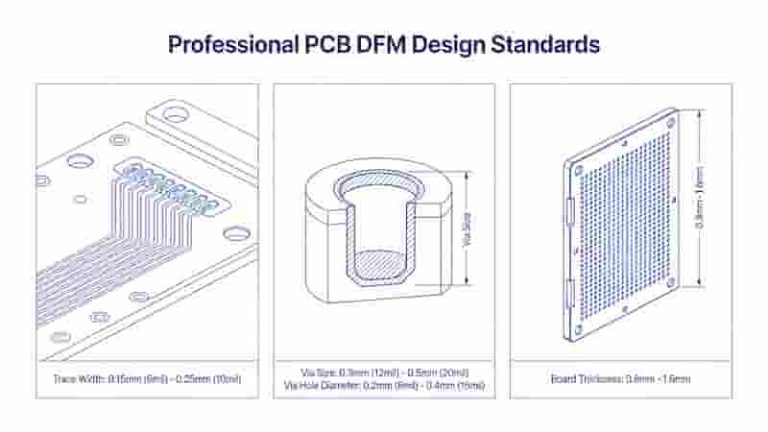
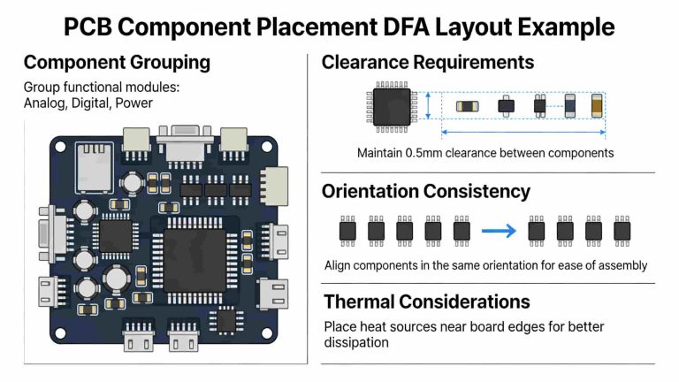
- PCB dimensions and component layout
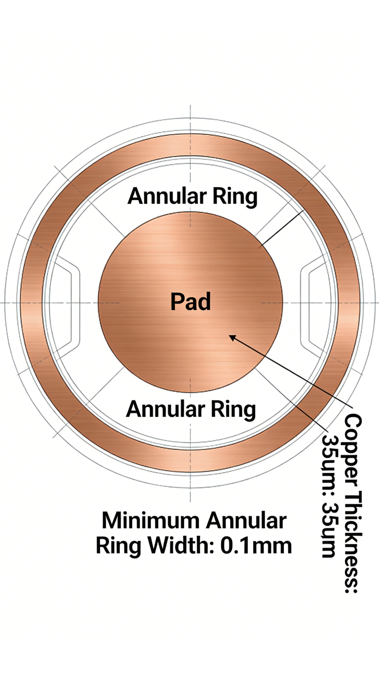
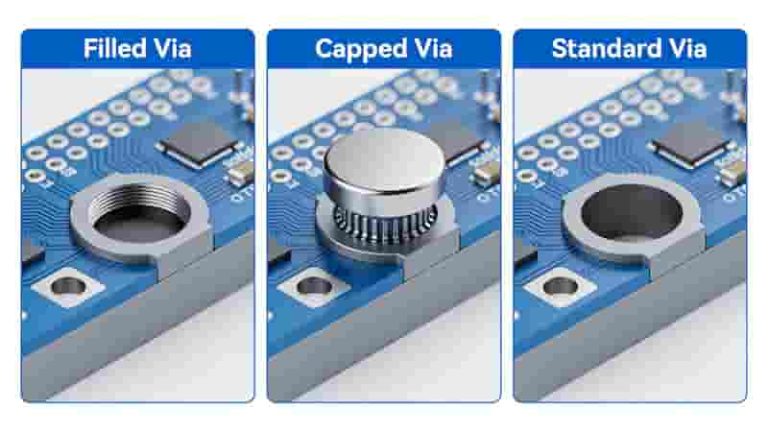
- Component selection and pad and through-hole design
- Process edges, fiducials, and positioning features
- Mechanical assembly requirements
Generated DFM reports document design issues like ISO9001 audit reports, clearly listing non-conformities, root causes, and correction requirements. These reports are created continuously throughout the design process.

III. The Significance of Manufacturability Analysis
1. Enhanced Design Verification and Production Yield
Electronic DFM software eliminates most PCB processing and assembly issues early in design, reducing redesign iterations and schedule delays. It improves right-first-time success rates, minimizes quality risks, and lowers long-term maintenance costs while significantly reducing inspection time from days to hours.
2. Improved Design Platforms
Integrating DFM software closes the loop between design and verification, complementing existing tools for schematic design, component management, PCB layout, and simulation. This ensures design correctness, shortens cycles, and improves product reliability while reducing dependency on highly experienced technicians.
IV. Main Features of Manufacturability Analysis
Design and Manufacturability Synchronization
During PCBA layout, designers use DFM to analyze and correct issues in real time, reducing experience limitations and improving efficiency while avoiding post-development revisions.
Process and Design Synchronization
DFM connects design and production, providing early manufacturing feedback to optimize PCB designs for current production capabilities.
Material, Process, and Design Synchronization
DFM validates BOM data and document compatibility, simulating PCBA assembly to deliver precise production data unavailable through traditional reviews.
Implementing DFM transforms electronic product development, enabling engineering teams to identify manufacturing issues early. This predictive approach elevates R&D capabilities, achieves right-first-time production, reduces costs, shortens cycles, and improves overall product quality.
Guideline and Reference Materials
- IPC-2221(L)
- CPCP/JPCA-PCB01-2006
- IPC-4101
- IPC-D-300G
- IPC-A-600F
Related Resources
- Aspects of PCB Design For Manufacturing and Design For Assembly
- HDI PCB Layout and Basic HDI Design Guidelines
- Basic Knowledge of PCB Pad Design
- PCB Terminology Glossary
- PCB Design Software Free Download
- Five Factors for FPC PCB Impedance Control
- Custom Circuit Board Printing
Download the Design for Manufacturability Checklist
Design for Manufacturability Checklist_EN
Design for Manufacturability Checklist_zh
Conclusion
DFM and DFA are essential for creating reliable, cost-effective PCB assemblies. By implementing these principles early in design, manufacturers achieve higher yields, lower costs, and faster time-to-market while maintaining compliance with international quality standards.
Ready to Start Your PCB Projects
Get DFM-optimized boards in as fast as 24 hours. 100% quality guaranteed.
Get a Free Quote
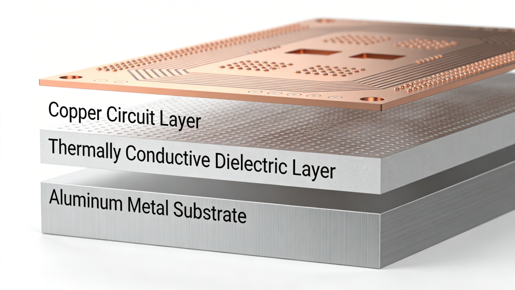
Professional Metal Core PCB (MCPCB) Manufacturing & Custom Service in China
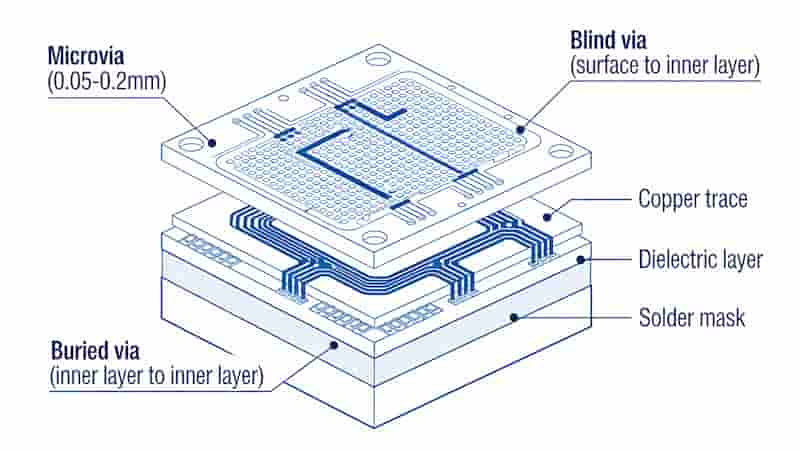
The Essentials of Microvias – Enabling Miniaturization in PCBs
Copper Core PCB vs. Metal Core PCB: Key Differences & Advantages
Complete Introduction of Flexible Circuit Board Materials
What is a Pad in PCB Design?