|

Rapid PCB Prototyping | Accelerate Innovation & Speed Up Time-to-Market

What Is Rapid PCB Prototyping Process Explanation

Rapid PCB prototyping delivers fast-turn fabrication from 8 hours for double-sided boards to 24–72 hours for multilayer prototypes. We provide high-quality, IPC Class 2, RoHS & UL certified services to accelerate your product development.

Why Choose Our Rapid PCB Prototyping

In the fast-paced electronics industry, speed and quality are critical. We specialize in professional rapid PCB prototyping and fast‑turn fabrication to help engineers, R&D teams, and enterprises launch products faster.

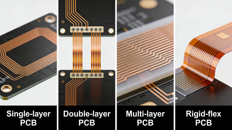
  • Full PCB types: single‑sided, double‑sided, multilayer, rigid, flexible & rigid‑flex
  • Ultra‑fast lead times: 8 hours for double‑sided prototypes; 24–72 hours for small batches
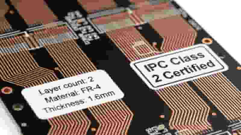
  • High quality: IPC Class 2, RoHS and UL certified
  • Low MOQ: 5–100 pieces for iterative design testing
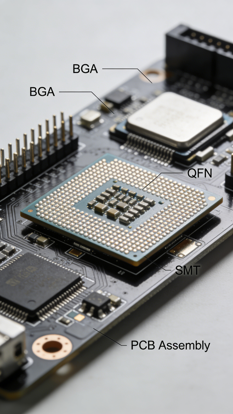
  • One‑stop service: PCB manufacturing + SMT/THT assembly + component sourcing

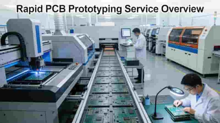
Rapid PCB Prototyping Service Overview for Industrial Engineers

What Is Rapid PCB Prototyping

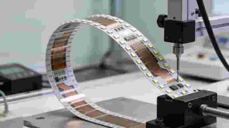
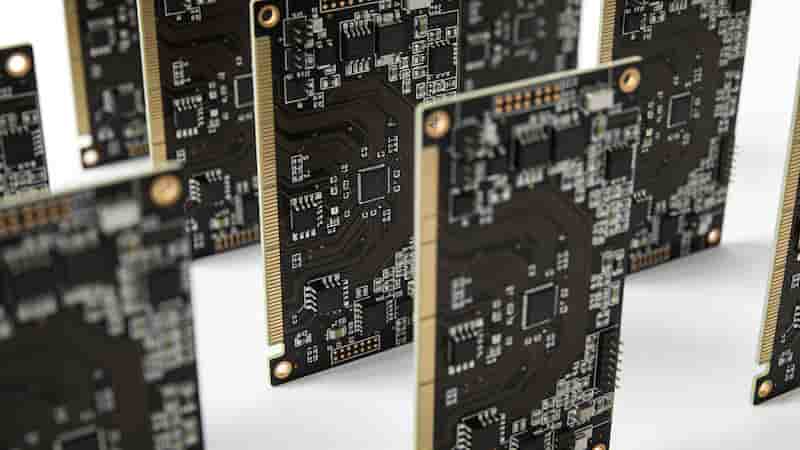
Rapid PCB prototyping produces small‑batch printed circuit boards to test and validate designs before mass production. It helps engineers detect flaws early and ensure final products meet performance and reliability standards.

Speed

Prototypes as fast as 8 hours for double‑sided PCBs, 24–72 hours for multilayer boards.

Flexibility

Supports complex designs including multilayer PCBs with blind or buried vias.

Cost Efficiency

Reduce expensive mass‑production revisions by validating designs early.
What Is Rapid PCB Prototyping Process Explanation

Benefits of Fast-Turn PCB Prototyping

Our rapid PCB prototyping service helps you stay competitive and build better products with less risk.

  • Speed Up Time-to-Market: Launch products faster with 8-hour quick‑turn prototypes
  • Ensure Flawless Designs: Test and optimize early to avoid production failures
  • Maintain High-Quality Standards: IPC Class 2, RoHS & UL compliant for industrial use
  • Reduce Total Costs: Low MOQ and fewer revisions lower overall development cost
  • Support Complex Customization: Multilayer, flexible, rigid‑flex and high‑precision designs

Key Benefits of Rapid PCB Prototyping for Global Buyers

Why We Stand Out

  • Advanced Equipment: Automated production lines ensure precision and fast delivery
  • Professional Engineering: Free Gerber review & DFM optimization suggestions
  • Global Service: Reliable delivery to USA, Canada, UK, Europe, Australia & worldwide
  • 24/7 Support: Fast response to all your inquiries and project needs

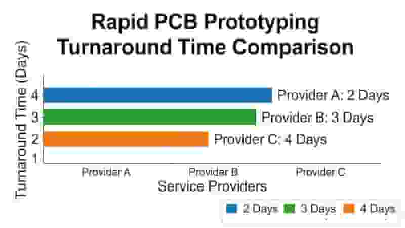
Rapid PCB Prototyping Turnaround Time

Layers≤0.1㎡Normal0.1‑1㎡Normal1‑2㎡Normal
Single-layer24H3 Days24H4 Days3 Days5 Days
Double-layer24H4 Days2 Days5 Days3 Days7 Days
4 Layer2 Days6 Days3 Days7 Days4 Days8 Days
6 Layer3 Days7 Days4 Days8 Days5 Days10 Days
8 Layer3 Days9 Days4 Days10 Days6 Days11 Days
Rapid PCB Prototype Lead Time and Production Capacity Table

How to Get Started

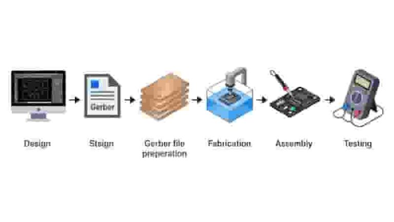
  1. Prepare Gerber files and specify layer count, quantity and delivery requirements
  2. Email us for a free, fast quotation based on your needs
  3. Choose expedited rapid PCB prototyping service
  4. Full quality inspection following international standards
  5. Fast global delivery to your door

Summary

Rapid PCB prototyping is essential for modern electronics development. We combine ultra‑fast lead times, strict quality control, low MOQ, and professional support to help you innovate faster and reduce risks.

Request Your Rapid PCB Prototyping Quote

Get DFM‑optimized boards in as fast as 24 hours. 100% quality guaranteed. Send your Gerber files now for an instant quote.

Get a Free Quote Now

PCB storage environment temperature humidity IPC standard control

How to Store PCB and PCBA? Complete IPC Storage Guidelines
Posted on
0 Comments
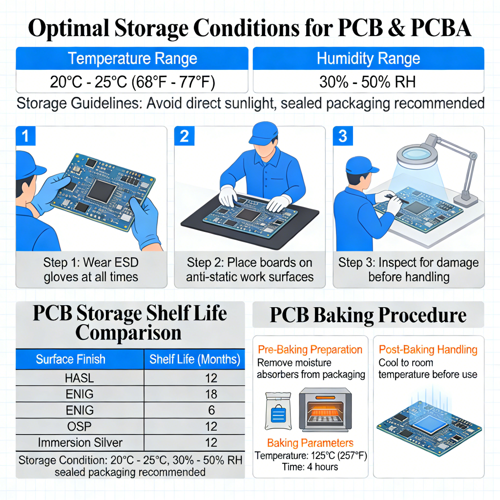
Learn PCB storage and PCBA storage best practices to avoid oxidation, ESD, moisture damage, and ensure reliable performance for industrial electronics. PCB storage and PCBA storage are critical for manufacturers and buyers alike. Proper storage prevents damage, maintains solderability, and avoids costly failures during assembly or operation. After production, boards are stored with strict precautions…
Laser cutting nano coating SMT PCB stencil production process

Nano-Coated PCB Stencil Manufacturing for Precision & Durability

Posted on
0 Comments
Discover industry-leading performance with our nano-coated PCB stencils. Engineered to support high-precision SMT printing processes, professional nano surface treatment greatly improves stencil durability, stabilizes solder paste deposition quality, and cuts routine maintenance workload, helping your entire PCB assembly line run stably and efficiently. Why Choose Nano-Coated PCB Stencils For SMT Production Nano-coated SMT stencils deliver…
PCBA finished product storage conditions SMT PCB assembly

How Long Can PCBA Finished Products Be Stored?

Posted on
0 Comments
PCBA finished products can typically be stored from 3 months to 10 years under controlled conditions, depending on surface finish, packaging, components, and environment. This guide explains official shelf life standards, storage conditions, and best practices for industrial buyers and engineers. What Is PCBA (PCB Assembly)? PCBA stands for Printed Circuit Board Assembly, the completed…
PCB Order Process Flow for Prototyping Fabrication Assembly

How to Order PCB Prototyping, Fabrication & Assembly Services in China

Posted on
0 Comments
Get a clear quote within 24 hours and receive high-quality PCB prototypes in as fast as 3-5 days, with one-to-one engineering support from inquiry to delivery. Get a Free Quote Now 24h quotation · 3-5 day PCB prototyping · One-stop PCB & PCBA Why Engineers and Buyers Choose Us From fast PCB prototypes to full…
Step Stencil vs Standard Stencil Comparison PCB SMT Production

Step Stencils: Precision Solutions for Modern PCB Assembly

Posted on
0 Comments
Step stencils optimize solder paste deposition for mixed-component PCBs, improving yield, reliability, and first-pass success in SMT assembly for electronics, automotive, and medical devices. Imagine a production line where tiny 01005 components sit alongside large edge connectors on a single printed circuit board. The challenge? Applying just the right amount of solder paste to each…
6Layer PCB Stack up

6 Layer PCB Guide: Stackup, Thickness, Design & Competitive Price

Posted on
0 Comments
A 6 Layer PCB Board comprises three dielectric layers (insulating layers) and three conductive layers. The dielectric layers are usually made of fiberglass (a common material in PCB manufacturing) or other high-performance insulating materials, which provide electrical insulation between layers. Meanwhile, the conductive layers are typically composed of copper foil—with common thicknesses ranging from 0.5oz…

FAQs About Rapid PCB Prototyping

A: Double-sided PCBs can be finished in 8 hours. Multilayer prototypes take 24 to 72 hours based on layer count and board size.

A: We offer single-sided, double-sided, multilayer, rigid, flexible and rigid-flex PCBs, including boards with blind and buried vias.

A: All products comply with IPC Class 2, RoHS and UL standards to meet industrial quality requirements.

A: The MOQ ranges from 5 to 100 pieces, ideal for design iteration and small-batch testing.

A: We provide SMT & THT assembly and component sourcing, delivering complete one-stop solutions.

A: It shortens time-to-market, detects design defects early, lowers revision costs and supports complex customized designs.

A: Lead time depends on PCB layer count and board area. Larger size and more layers will extend the delivery period accordingly.

A: Yes. Our professional engineers offer free Gerber file checking and DFM suggestions to avoid production risks.

A: Send Gerber files and requirements → Get free quote → Confirm order → Production & full inspection → Global delivery.

Similar Posts