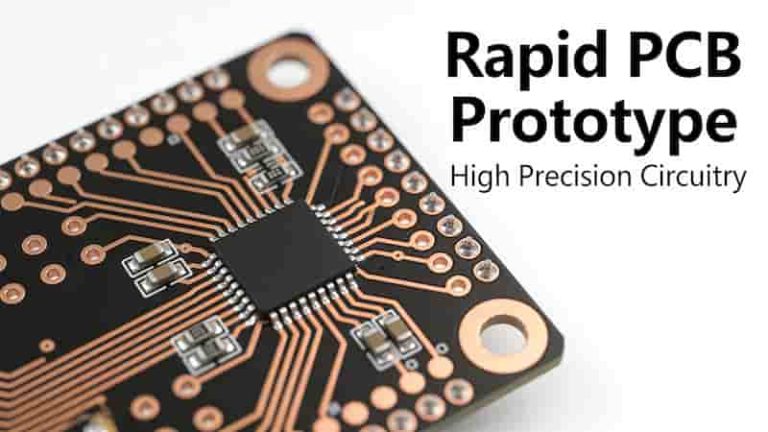
Summary: Master critical standards for PCB prototype manufacturing including file formats, design rules, layer stackup, and documentation. Optimize your prototyping workflow with expert best practices to achieve high-quality, cost-effective, and on-time PCB prototypes for industrial and engineering applications.
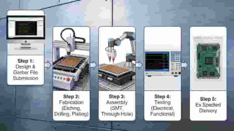
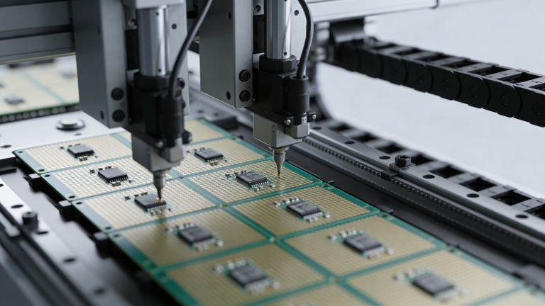
Prototype PCB Fabrication
PCB prototyping is a crucial step in the electronics design process, enabling designers to validate circuits and product concepts efficiently and cost-effectively. To ensure high-quality prototype boards are delivered on time, understanding the requirements for PCB prototype manufacturing is critical. By providing your manufacturing partner with precise files, adhering to design rules, and supplying comprehensive documentation, you can avoid delays and errors, setting your project up for success.
This article outlines the essential requirements for PCB prototype manufacturing, from file formats to layer stackup specifications, with practical tips and industry insights to streamline your prototyping process. Whether you are pursuing standard or quick-turn fabrication, these guidelines will help you achieve optimal results.
Choosing the Right Type of PCB
Selecting the appropriate PCB type is the foundation of a successful prototype. Different PCB types cater to specific applications, and understanding their characteristics ensures your design meets performance and cost requirements.
Rigid PCB
Rigid PCBs, made from solid substrates like FR-4, are the most common and cost-effective option. Their rigid structure prevents bending, making them ideal for applications such as desktop computers and industrial equipment where structural integrity is crucial.
Flexible PCB
Flexible PCBs, constructed from materials like polyimide or polyester film, can bend and conform to unique shapes. They are widely used in compact devices such as wearable electronics, cameras, and UAVs. Our team used flexible PCB to fit a curved housing, reducing the device’s footprint by 15%.
Rigid-Flex PCB
Rigid-flex PCBs combine rigid and flexible layers, offering versatility for complex designs. They are common in aerospace and medical devices where reliability and space savings are critical.
HDI PCB
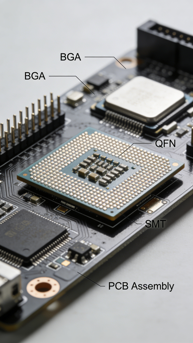
High-Density Interconnect (HDI) PCBs feature compact designs with microvias (typically less than 0.15 mm in diameter) and dense circuitry. Essential for modern devices like smartphones and 5G equipment, where high-frequency signals demand minimal transmission loss.
Other PCB Types
Specialty PCBs, such as LED PCBs, Aluminum PCBs, and High-TG PCBs, cater to niche applications like high-power lighting or high-temperature environments.
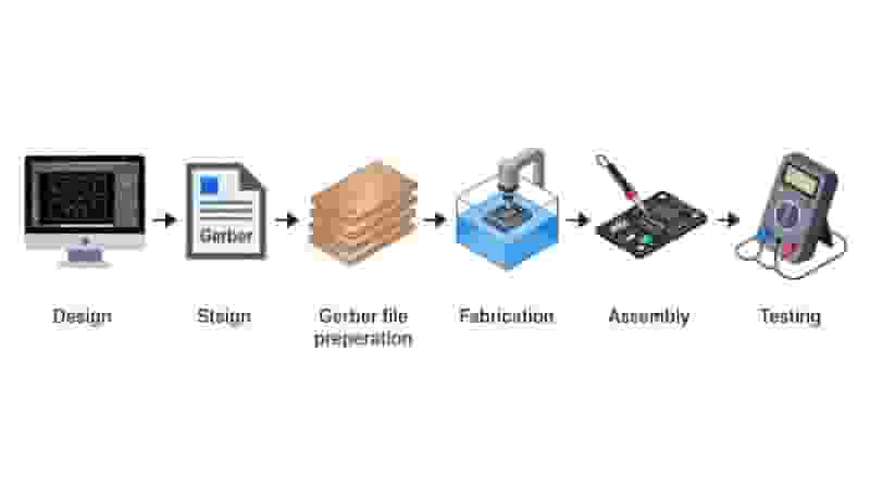
File Formats for PCB Prototyping
Submitting the correct file formats ensures your PCB prototype manufacturing partner can accurately produce your prototype. Below are the primary formats accepted by most prototyping companies.
Gerber Files
Gerber files (RS-274X) are the industry standard, including copper layers, solder mask, silkscreen, and drill data. Verify files with a Gerber viewer before submission.
CAD Files
Native CAD files from Altium, Eagle, KiCad streamline workflows when supported by your manufacturer.
PDF Files
PDFs are suitable only for simple, low-density designs; avoid for complex prototypes.
Pro Tip: Include a README file to clarify contents and design intent.

Key PCB Design Rules to Follow
Adhering to design rules ensures your PCB prototype manufacturing output is manufacturable and reliable.
- Trace Width/Spacing: Min 0.006 inch (0.15 mm) for standard 1 oz copper
- Annular Rings: Min 0.004 inch (0.1 mm) to prevent pad lifting
- Via Sizes: 0.2-0.3 mm finished diameter for reliable plating
- Silkscreen Margins: Min 0.003 inch (0.076 mm) clearance to avoid bleeding
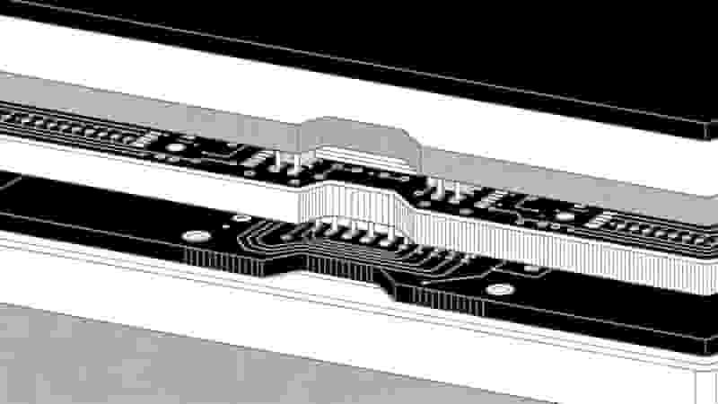
Specifying Layer Stackup Requirements
Layer stackup defines electrical and mechanical performance for PCB prototype manufacturing.
- Layer Count: 2, 4, 6+ based on routing complexity
- Materials: FR-4, polyimide, Rogers for high-frequency
- Thickness: Standard 1.6 mm; 0.8 mm for compact designs
- Copper Weight: 1 oz standard, 2 oz for high current
Panelization for Cost Efficiency
Panelization lowers costs for mid-volume prototypes. Include tooling holes and mouse bites for clean separation.
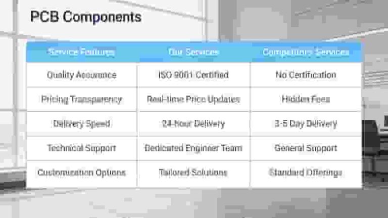
Essential Documentation for Prototyping
- Bill of Materials (BOM): Full part numbers, values, quantities
- Assembly Drawings: Placement, stackup, tolerances, special notes
- Test Procedures: Continuity, electrical, functional criteria
- Finish & Color: Solder mask, surface finish (HASL, ENIG, OSP)
Understanding Lead Times
Standard lead times: 10-14 days; expedited: 24-48 hours. Always include DFM check (1-2 days) in your timeline.
Common Pitfalls and How to Avoid Them
- Incorrect Gerber files: Validate with a viewer
- Incomplete documentation: Provide full BOM and drawings
- Ignoring DFM feedback: Resolve issues early
Conclusion
Success in PCB prototype manufacturing depends on accurate files, strict design rules, clear layer stackup, complete documentation, and proactive DFM review. These practices reduce errors, lower costs, and speed up validation for mass production.
Need Professional PCB Prototype Manufacturing?
We provide fast-turn, high-precision PCB prototype manufacturing for global engineers and industrial buyers. Get free DFM checks, full testing, and on-time delivery for your custom projects.
Request a Free Quote
|
Contact Us for Custom Solutions