|

What is a PCB Manufacturer? The Definitive Guide

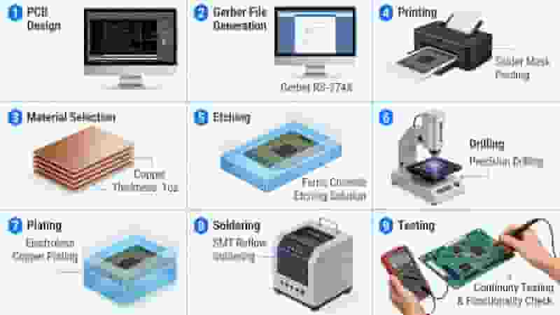
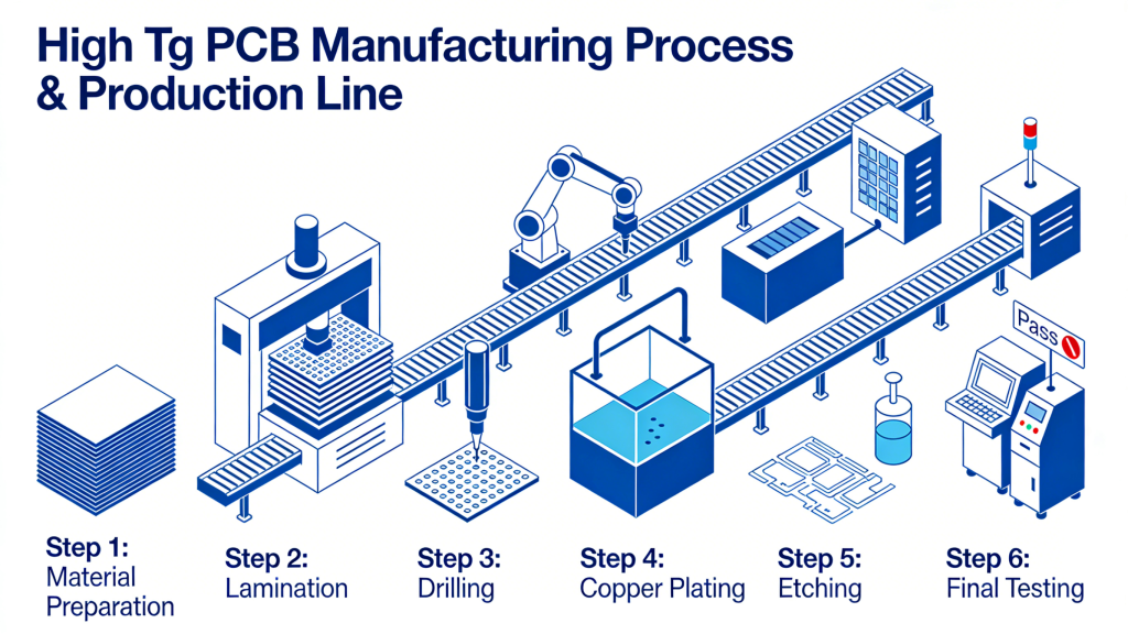
Full PCB manufacturing process from design to finished circuit boards

A PCB manufacturer is a specialized enterprise that designs, produces, tests, and supplies printed circuit boards for global electronics industries. This definitive guide explains core roles, manufacturing processes, advanced technologies, service ranges, and how to select a reliable PCB manufacturer for industrial, automotive, medical, and telecom applications.

Role & Responsibilities of a PCB Manufacturer

A PCB manufacturer serves as a critical link in the global electronics supply chain, turning electronic design files into physical, reliable circuit boards.

Key responsibilities include engineering support, precise fabrication, strict testing, quality control, and secure global logistics.
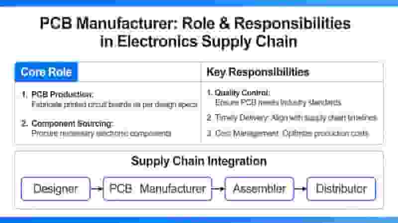
PCB manufacturer role and responsibilities in electronics supply chain

1. Design & Engineering Support

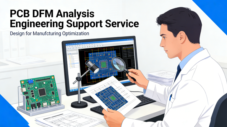
Professional PCB manufacturer teams provide DFM analysis, optimize layouts, and ensure designs are producible with high yield.

2. Core PCB Fabrication

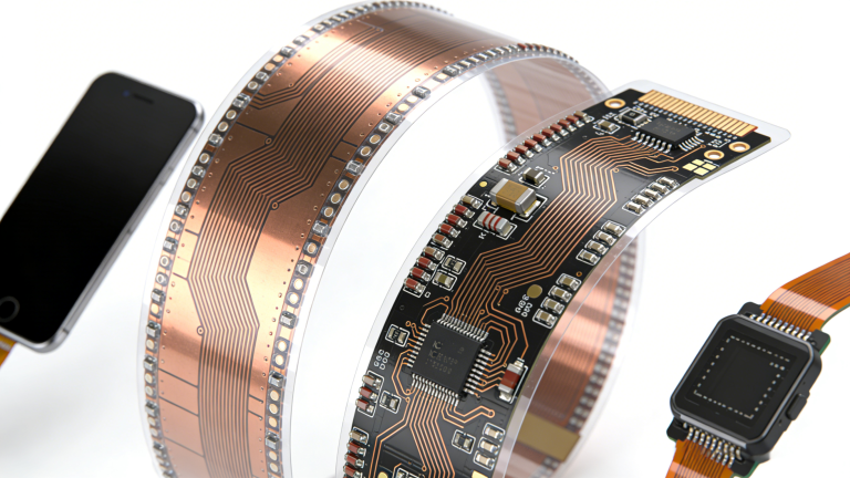
We produce rigid, flex, rigid-flex, HDI, metal-core, and high-frequency PCBs with strict adherence to IPC and UL standards.

3. Testing & Quality Inspection

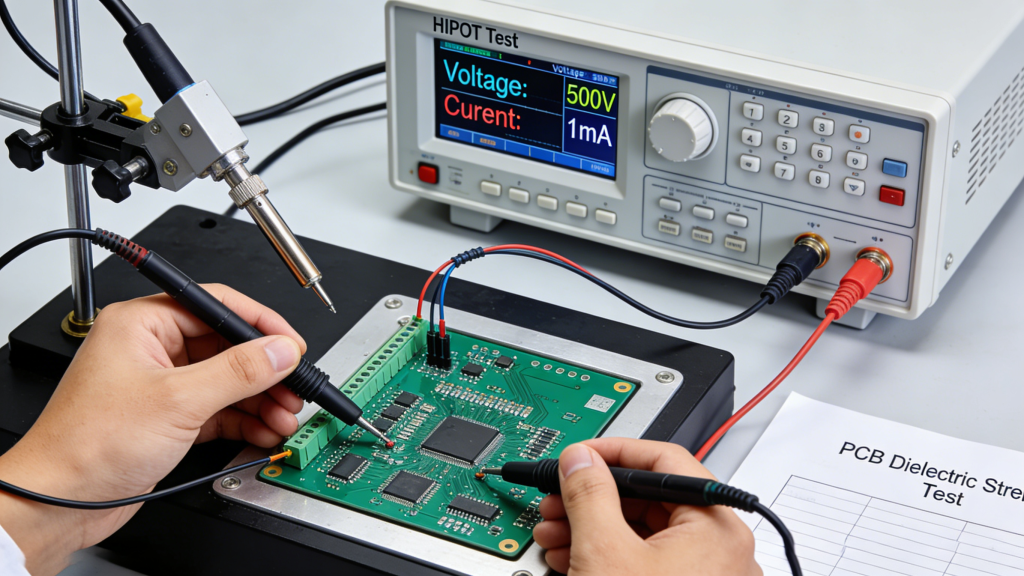
Full inspection includes AOI, flying probe testing, electrical testing, solder mask verification, and dimensional checks.

4. Supply Chain & Global Delivery

Stable raw material supply, efficient production planning, and safe international shipping support your project schedule.

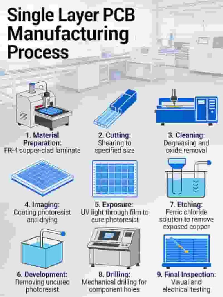
Full PCB Manufacturing Process

The complete process from design to finished boards ensures every PCB meets performance and reliability requirements.

  1. Design file review & DFM analysis
  2. Material cutting & preparation
  3. Drilling & desmear
  4. Electroless copper & plating
  5. Imaging & etching
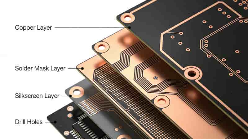
  6. Solder mask & silkscreen
  7. Surface finishing (ENIG, HASL, OSP, etc.)
  8. AOI & electrical testing
  9. Profile, V-cut, cleaning & packaging
Full PCB manufacturing process from design to finished circuit boards

Advanced Technologies in PCB Manufacturing

Top PCB manufacturer facilities use modern equipment to produce high-precision boards for demanding industries.

Fabrication Technologies

Direct imaging, plasma etching, laser drilling, and automated plating lines support HDI and high-frequency PCB production.

High-Performance Materials

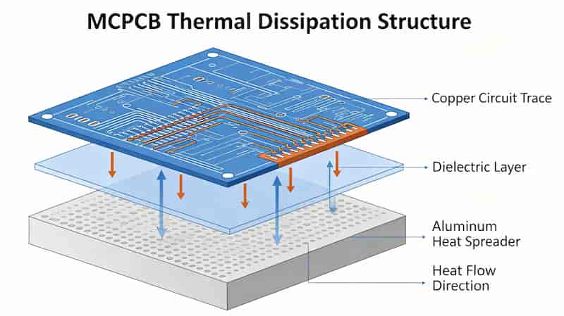
High-speed laminates, low-loss materials, aluminum substrates, and flexible base materials expand application possibilities.

Testing & Inspection

AOI, 3D X-ray, flying probe testers, and thermal stress testing guarantee long-term reliability.
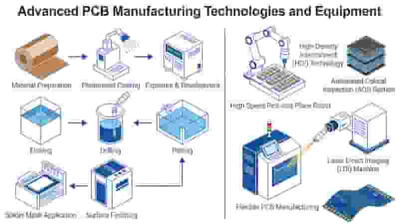
Advanced PCB manufacturing technologies and equipment

Complete Service Offerings

A full-service PCB manufacturer supports prototyping to mass production for global buyers.

  • Prototype PCB & quick-turn services
  • Small-batch & mass production
  • HDI, rigid-flex, high-frequency, metal-core PCBs
  • DFM engineering support
  • Full electrical & reliability testing
  • Global export packaging & logistics
ItemStandard PCBAdvanced PCB
Layers1–8 layers8–30+ layers, HDI
ApplicationsConsumer, industrialAutomotive, medical, aerospace
CertificationsISO 9001, IPC-A-600ISO 9001, IATF 16949, UL, RoHS

How to Select a Reliable PCB Manufacturer

When choosing a PCB manufacturer for global projects, focus on these critical factors:

  1. Proven technical capabilities and equipment
  2. Strict quality system and international certifications
  3. Stable lead times and production capacity
  4. Professional engineering and customer support
  5. Transparent pricing and cost efficiency
  6. Strong export and logistics experience
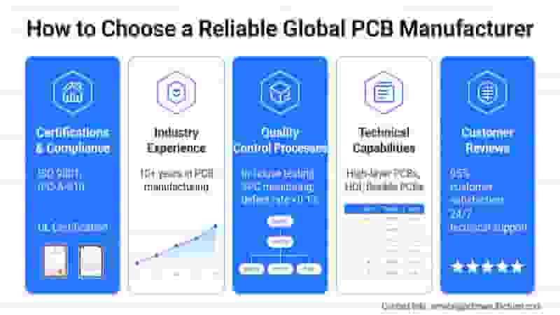
How to choose a reliable global PCB manufacturer

Conclusion

A trusted PCB manufacturer delivers consistent quality, technical expertise, and reliable global supply. Whether you need prototypes, small batches, or mass production, partnering with an experienced export-focused PCB manufacturer ensures your electronic projects succeed.

Get Your PCB Solution Now

Request a free quote, DFM analysis, or custom PCB manufacturing support from our expert team.

Inquiry Now
Get Free Quote
HDI PCB Microvia, Blind & Buried Via Structure

HDI PCB Manufacturing – Microvia, Blind & Buried Via HDI Boards up to 30 Layers

HDI PCB manufacturing provides high-density interconnect solutions with microvia, blind via, and buried via structures for compact, high-performance electronics. We deliver reliable HDI boards from prototype to mass production, supporting up to 30 layers for automotive, 5G, medical, and industrial applications. What Is HDI PCB and Why Choose It High-density interconnect (HDI) PCBs offer much…
Laser cutting nano coating SMT PCB stencil production process

Nano-Coated PCB Stencil Manufacturing for Precision & Durability

Discover industry-leading performance with our nano-coated PCB stencils. Engineered to support high-precision SMT printing processes, professional nano surface treatment greatly improves stencil durability, stabilizes solder paste deposition quality, and cuts routine maintenance workload, helping your entire PCB assembly line run stably and efficiently. Why Choose Nano-Coated PCB Stencils For SMT Production Nano-coated SMT stencils deliver…
HDI PCB structure cross section with microvias and fine traces

HDI PCB Layout and Basic HDI Design Guidelines 

This professional guide covers HDI PCB layout practices, stack-up, microvias, routing rules, DFM, impedance control and IPC standards to help engineers and procurement teams build reliable, mass-producible HDI PCB for high-speed, miniaturized electronics. What Is HDI PCB Layout HDI PCB (High-Density Interconnect) layout refers to design methods used when trace widths drop below 8 mils…
FR-4 PCB material definition and flame retardant standard

What is FR-4 Material in PCB Fabrication? The Complete Engineering Guide

FR-4 is the global industry-standard flame-retardant glass-reinforced epoxy laminate for rigid PCB fabrication. This guide explains definition, composition, properties, grades, selection, and why FR-4 PCB is the top choice for engineers and global buyers. What is FR-4 Material? FR-4 (Flame Retardant Type 4) is a NEMA-defined material grade for flame-resistant epoxy laminates. It is not…
Flex PCB wearable medical aerospace application

Rigid PCB vs Flex PCB: Key Differences, Applications & Selection Guide

PCBs are the backbone of modern electronics. While Rigid PCB and Flex PCB serve similar core functions, they differ greatly in materials, flexibility, cost, durability, and ideal use cases. This professional guide helps engineers and buyers choose the right PCB for industrial and export projects. Printed Circuit Boards (PCBs) are the backbone of modern electronics,…
PCB Component Spacing vs Height Layout Guidelines

PCB Pad Design Basics: Standards, Rules & Best Practices for Engineers

This guide covers core PCB pad design principles, component spacing, IPC standards, SMD/through-hole rules, thermal management, and DFM to boost assembly yield, reliability, and performance for industrial and export-grade PCBs. PCB Component Layout & Spacing Rules When laying out PCB components, designers must balance minimum component spacing against component height and thickness. Proper spacing prevents…

FAQs About PCB Manufacturer & Manufacturing Services

A: A PCB manufacturer converts design files into finished circuit boards, covering engineering support, fabrication, testing, quality control and global delivery.

A: We provide PCB prototyping, small-batch & mass production, DFM analysis, full testing and one-stop PCBA assembly solutions.

A: We make rigid, flex, rigid-flex, HDI, metal-core and high-frequency PCBs to suit different industrial demands.

A: DFM review → Material preparation → Drilling & plating → Imaging & etching → Solder mask & silkscreen → Surface finish → Testing → Cutting & packaging.

A: We use laser drilling, direct imaging and plasma etching. Testing includes AOI, 3D X-ray, flying probe and thermal stress test.

A: Standard PCBs have ISO 9001 and IPC-A-600. Advanced boards for automotive and medical also support IATF 16949, UL and RoHS.

A: Check technical strength, certifications, delivery stability, engineering support, pricing and overseas logistics capability.

A: Prototypes take 3–7 days, and mass production needs 7–15 days, depending on PCB complexity.

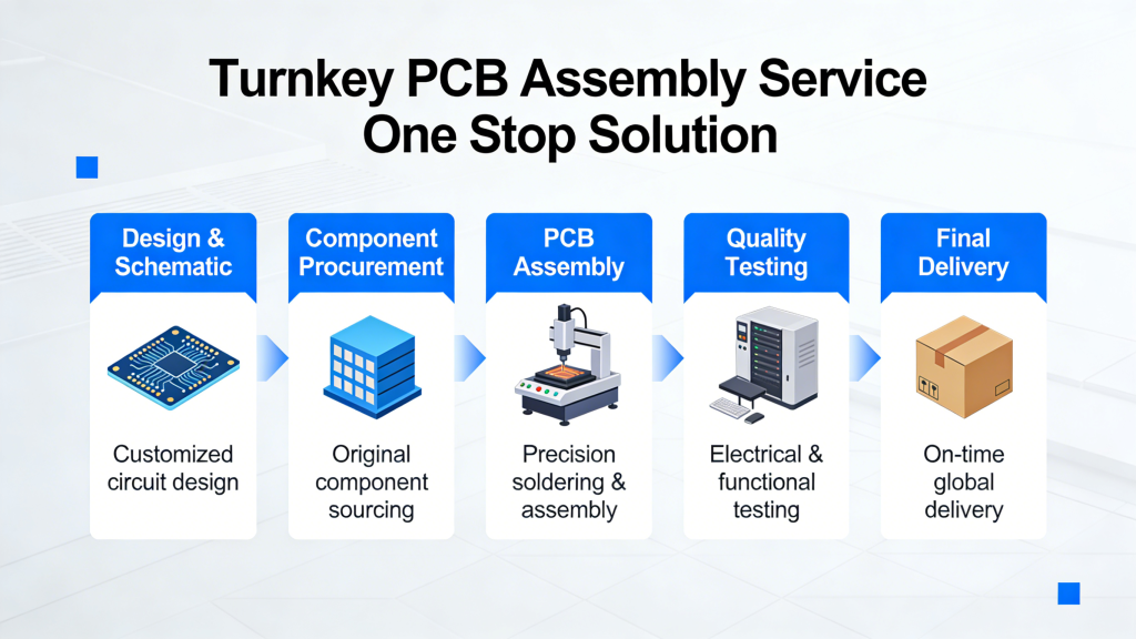
A: Yes, we provide supporting PCBA turnkey services to meet one-stop manufacturing requirements.

Similar Posts