Dielectric strength is critical for PCB reliability, ensuring insulation and safety in high-voltage and high-frequency applications. This guide dives into key PCB materials, their dielectric properties, testing techniques, influencing factors, and practical advice for designing robust circuits.
Introduction
In the fast-paced world of electronics, a single oversight in PCB design can lead to catastrophic failure—like a high-voltage power supply short-circuiting in an electric vehicle due to insufficient dielectric strength. This critical property determines whether a PCB can withstand the electrical stresses of its environment, ensuring safety, reliability, and performance.
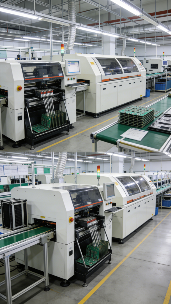
We are a trusted China-based manufacturer of PCBs (including prototypes, single-sided, double-sided, multilayer, rigid, flexible, and rigid-flex) and assembly services (SMT, THT, mixed technology, turnkey, and component sourcing). This guide empowers engineers, designers, and purchasers with a deep understanding of PCB dielectric strength, free from promotional fluff.
What is Dielectric Strength in PCBs?
Dielectric strength measures a material’s ability to resist an electric field without breaking down, expressed in volts per mil (V/mil) or kilovolts per millimeter (kV/mm). In PCBs, dielectric materials prevent unwanted current flow, ensuring electrical isolation, signal integrity, and safety.
When dielectric strength is exceeded, the material undergoes electrical breakdown, causing arcing, short circuits, or permanent damage. PCB dielectric strength is governed by IPC-4101 and UL standards to ensure compliance.
Key Related Properties
Dielectric Constant (Dk): Measures energy storage, critical for high-frequency signals.
Dissipation Factor (Df): Indicates energy loss, affecting RF signal clarity.
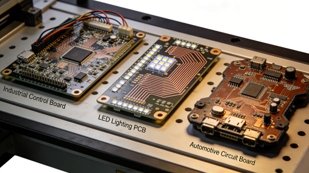
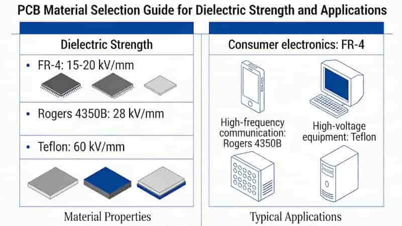
Common PCB Materials and Their Dielectric Strengths
The substrate defines a PCB’s insulation foundation. Below are the most widely used materials and their dielectric strength values for industrial and export applications.
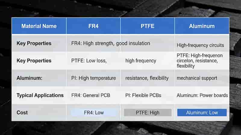
PTFE (Teflon / Rogers)
Dielectric Strength: 500–700 V/mil (20–28 kV/mm)
Applications: RF, microwave, 5G, radar, high-frequency circuits
Pros: Ultra-low loss, high thermal stability, excellent signal integrity
PI (Polyimide / Kapton)
Dielectric Strength: 300–500 V/mil (12–20 kV/mm)
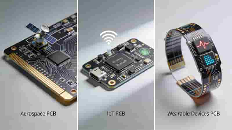
Applications: Flexible PCBs, rigid-flex, aerospace, medical, wearables
Pros: Flexible, heat-resistant up to 400°C, reliable in dynamic environments
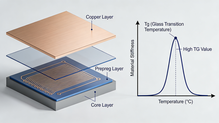
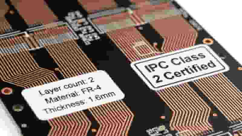
FR‑4 (Standard & High‑Tg)
Dielectric Strength: 300–500 V/mil (12–20 kV/mm)
Applications: General electronics, industrial controls, consumer devices
Pros: Cost-effective, widely available, stable for standard voltages
Ceramics
Dielectric Strength: 100–200 V/mil (4–8 kV/mm)
Applications: Automotive, aerospace, high-voltage power systems
Pros: Extreme temperature resistance, high durability
Metal‑Core Dielectric
Dielectric Strength: <100 V/mil (~4 kV/mm)
Applications: LEDs, power electronics, thermal management
Pros: Excellent heat dissipation for high-power devices
| Material | Dielectric Strength | Typical Applications |
|---|---|---|
| PTFE | 500–700 V/mil | RF, 5G, high-frequency |
| Polyimide (PI) | 300–500 V/mil | Flex, rigid-flex, aerospace |
| FR‑4 | 300–500 V/mil | General industrial & consumer |
| Ceramics | 100–200 V/mil | High-voltage, automotive |
| Metal-Core Dielectric | <100 V/mil | LED, power thermal management |
PCB Materials and Dielectric Strength Comparison Table
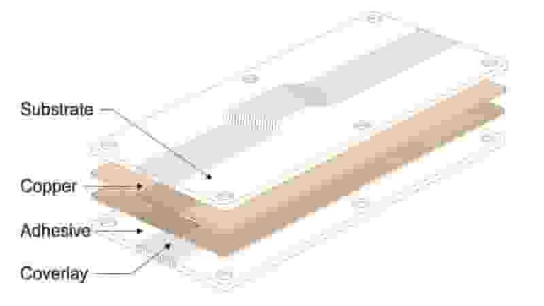
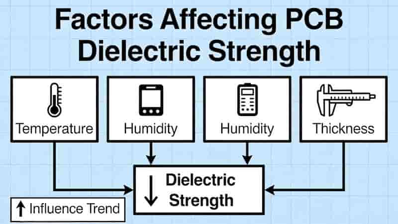
Factors Affecting Dielectric Strength in PCB Materials
Many factors influence the dielectric strength of PCB materials beyond base composition. Understanding these helps avoid insulation failure.
1. Material Composition & Quality
Molecular structure, resin type, fillers, and homogeneity directly determine intrinsic dielectric strength. High-grade resins and uniform lamination significantly improve performance.
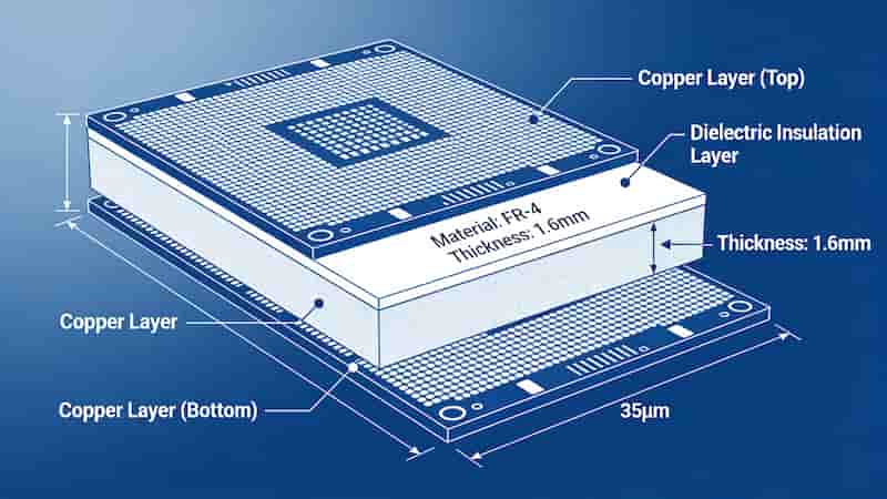
2. Dielectric Layer Thickness
Thicker dielectric layers increase breakdown voltage. Designers must balance thickness, size, weight, cost, and impedance control for optimal PCB performance.
3. Environmental Conditions
Temperature: High temperatures reduce dielectric performance, especially in FR‑4.
Humidity & Moisture: Absorbed water lowers insulation and raises breakdown risks.
Aging & Contamination: Dust, chemicals, and material degradation weaken insulation over time.
4. Manufacturing Quality
Voids, air pockets, uneven lamination, and impurities create weak points. Vacuum lamination and AOI inspection ensure stable dielectric strength in mass production.
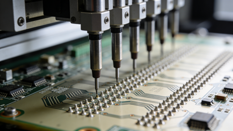
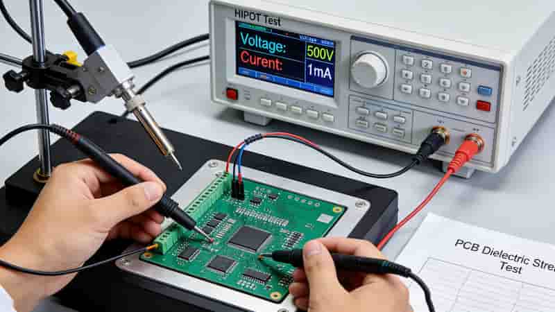
Dielectric Strength Testing for PCBs
Testing verifies that PCB materials meet required dielectric strength for safety and reliability. The HIPOT / Dielectric Withstand Voltage (DWV) test is the global industry standard.
Standard Testing Process
1. Connect test probes to PCB copper pads or test points
2. Gradually apply rated voltage (e.g., 1.5 kV) for 60 seconds
3. Monitor leakage current; a surge indicates breakdown
4. Record pass/fail against IPC‑9252 or UL requirements
Testing Standards & Tools
Standards: IPC‑9252, UL 746E, IEC 60664
Equipment: Dielectric strength tester, HIPOT tester
How to Select PCB Materials by Dielectric Strength
Choose the right PCB material by matching dielectric strength to your application’s voltage, frequency, environment, and budget.
• High-voltage systems (>1kV): PI, ceramics, high‑Tg FR‑4
• High-frequency/RF: PTFE, Rogers low‑loss materials
• Flex/rigid‑flex: Polyimide (PI)
• General industrial: Standard FR‑4
• High-power thermal: Metal‑core dielectric
Conclusion
Dielectric strength is the foundation of reliable, safe, and long‑lasting PCB performance. Selecting the right PCB materials, controlling manufacturing quality, and performing valid dielectric testing directly prevent breakdowns, short circuits, and field failures.
For industrial, automotive, medical, and telecom applications, proper material selection based on dielectric strength ensures compliance, durability, and cost efficiency.
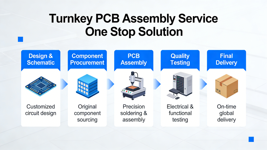
Get Your PCB Solution & Custom Quote
We provide professional PCB manufacturing, SMT assembly, and DFM support optimized for dielectric strength and reliability. Our ISO 9001, RoHS, and UL‑certified production ensures export‑grade quality for global buyers.
✔ Custom material selection for your voltage & frequency needs
✔ Free dielectric performance consultation
✔ Quick‑turn prototypes & mass production
✔ Full export support & global delivery
Contact Us for PCB Quote
© 2025 All Rights Reserved | Professional PCB Manufacturing & Assembly for Global Export
PCB Vias Explained: Through, Blind, and Buried Holes
Low-Cost PCB Assembly Service | Reliable Provider & Cheap PCB Solutions
UK PCB Prototype Manufacturing: Fast Turnaround, Cost-Effective & IPC-Certified Quality
Rapid PCB Prototyping | Accelerate Innovation & Speed Up Time-to-Market
Custom PCB Assembly Services for Low-Volume & Specialty Needs