A full professional overview of PCB vias including definitions, functions, types, manufacturing, reliability factors and advanced technologies for high‑performance multilayer printed circuit boards.
Introduction: Definition, Role, and Types of Vias in PCBs
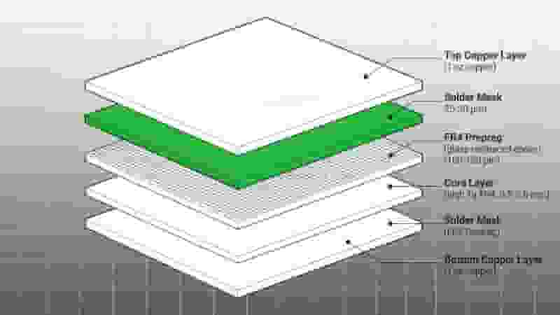
A via is a vertical electrical connection between layers in a printed circuit board. Vias enable traces to transition between layers to facilitate complex routing pathways and component connections within a confined PCB area or across multilayer PCB boards.
Vias play several important roles in PCBs. They provide vertical interconnections between copper layers, allowing signal traces and component leads to span between layers. Vias are also used strategically for shielding, heat transfer, grounding, and other functions. Additionally, component leads can be directly soldered into plated through-hole vias.
There are three major types of vias:
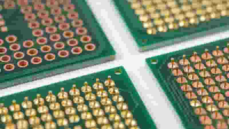
- Plated Through-hole Vias: Fully plated vias spanning the entire board vertically between layers. Plated through-hole vias (PTHs) enable robust layer transitions.
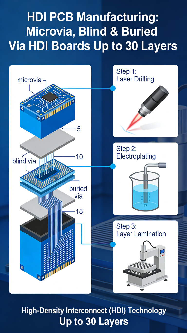
- Blind or Buried Vias: Partial-depth vias connecting internal layers without spanning fully through the board. Blind vias connect one internal layer to an external layer, while buried vias connect internal layers only.
- Micro Vias: Small diameter vias, typically below 0.15mm, created with laser drilling. Micro vias facilitate connections in high density PCBs.
The rest of this article provides an in-depth overview of everything related to PCB vias, including their functions, construction methods, reliability factors, and innovative via technologies that enable advanced PCB performance and designs.
What Are PCB Vias
A via is a plated vertical electrical connection that allows signals, power and ground to pass between layers in a multilayer printed circuit board. PCB vias are essential for creating compact, high‑density interconnect systems used in industrial electronics, automotive, 5G and high‑speed devices.
Core Functions of Vias in PCB
PCB vias support multiple critical roles beyond basic layer connection:
- Layer Interconnection: Enables vertical routing between multiple PCB layers
- Thermal Dissipation: Transfers heat from components to inner planes
- Grounding & Shielding: Reduces noise and stabilizes high‑speed signals
- Component Mounting: Provides secure connection for through‑hole parts
- High‑Density Routing: Supports miniaturization in HDI PCB designs
Main Types of PCB Vias
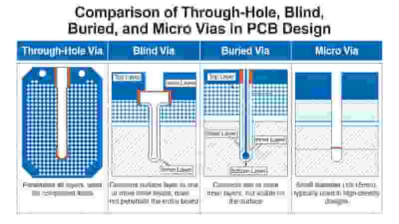
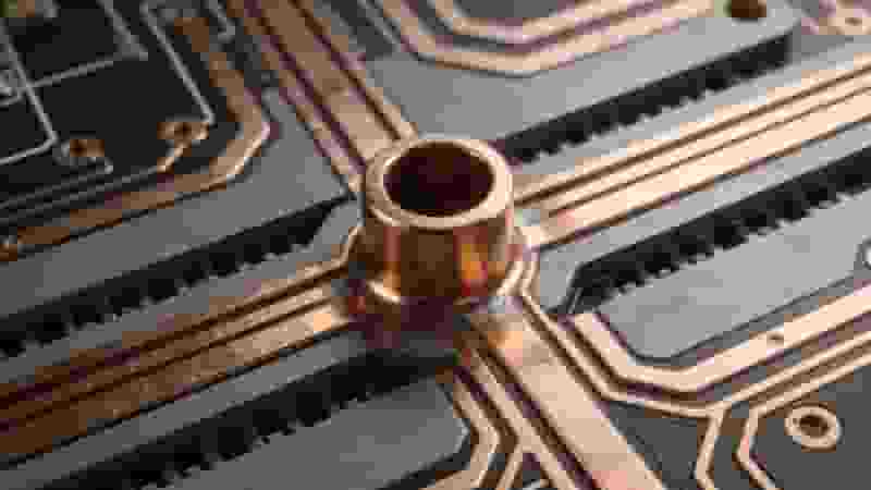
1. Plated Through‑Hole Vias (PTH)
Full‑depth vias that span the entire board thickness. Widely used in standard multilayer PCBs for reliable layer connections and component soldering.
2. Blind Vias
Connect an outer layer to one or more adjacent inner layers without going through the entire board. Improves routing density and signal quality.
3. Buried Vias
Connect only inner layers and are fully enclosed inside the PCB. Used in high‑layer‑count HDI boards to maximize routing space.
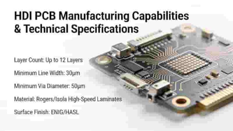
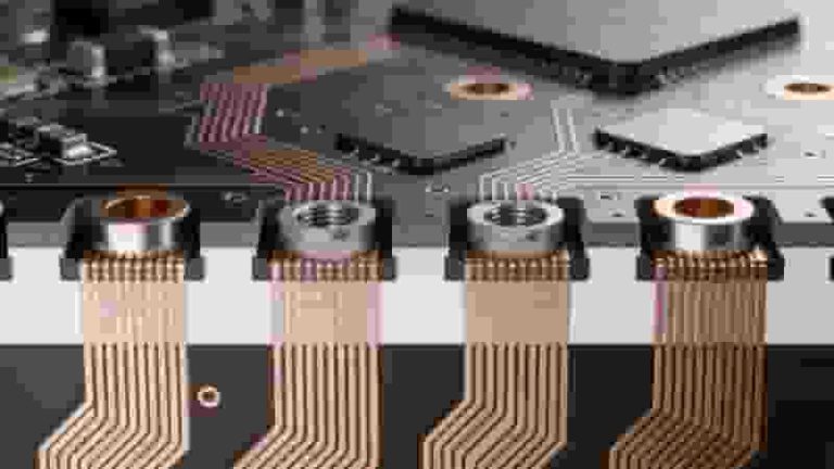
4. Micro Vias
Laser‑drilled vias typically ≤0.15 mm, designed for ultra‑high‑density interconnect PCBs used in 5G, mobile and automotive electronics.
| Via Type | Typical Size | Best Application | Cost Level |
|---|---|---|---|
| PTH Vias | 0.2 mm – 1.0 mm | General multilayer PCBs | Low |
| Blind / Buried Vias | 0.15 mm – 0.3 mm | Medium‑density boards | Medium |
| Micro Vias | ≤ 0.15 mm | HDI & high‑speed PCBs | High |
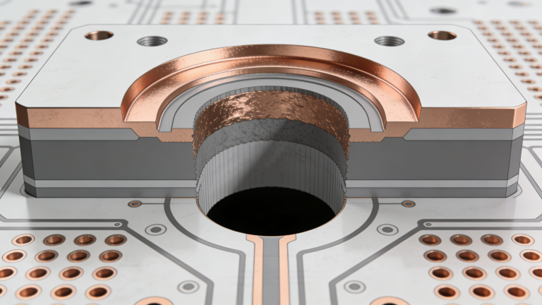
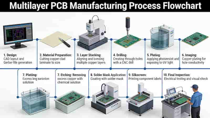
Via Manufacturing Process
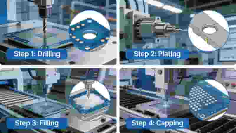
Precision manufacturing ensures stable and reliable PCB vias:
- Drilling: Mechanical or laser drilling for high precision
- Electroless Copper Plating: Forms conductive layer on hole walls
- Electroplating: Builds required copper thickness for conductivity
- Filling & Capping: Epoxy filling improves thermal and structural stability
- Solder Mask Application: Protects vias from oxidation and contamination
Via Reliability Considerations
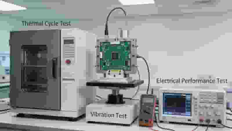
Common failure modes of PCB vias include barrel cracking, pad lifting, incomplete plating and solder joint failure. These issues are often caused by improper drilling, uneven plating, thermal expansion mismatch or excessive aspect ratio.
To improve via reliability, manufacturers control hole tolerance, optimize plating thickness, limit aspect ratio and use validated materials for PCB production.
Advanced Via Technologies
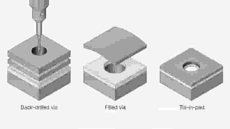
Back‑Drilled Vias
Remove excess stub to reduce signal resonance, ideal for high‑speed digital and RF PCBs.
Filled & Capped Vias
Improve heat transfer, prevent solder wicking and increase mechanical stability of PCB vias.
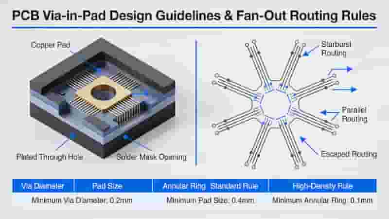
Via‑in‑Pad (VIP)
Embeds vias directly inside component pads to maximize routing density for BGA and fine‑pitch devices.
Tented Vias
Fully covered by solder mask for protection in harsh environments and high‑reliability PCBs.
Conclusion
PCB vias are foundational elements of modern printed circuit boards. They enable layer connectivity, thermal management, signal integrity and high‑density design. Choosing the right via type and controlling manufacturing quality directly affect the performance, lifespan and yield of PCB products.
With the development of 5G, automotive electronics and AI hardware, advanced via technologies will continue to evolve to support smaller, faster and more reliable PCB solutions.
Need Professional PCB & Via Manufacturing Support?
We specialize in high‑precision multilayer PCBs, HDI boards and reliable via fabrication for global industrial buyers and engineers.
Contact us for a free quote, DFM review or custom PCB solution today.
Request Your PCB Quote
Multilayer PCB Prototyping & Manufacturing Services | Fast & Reliable
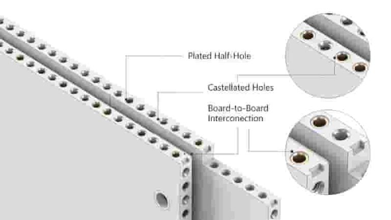
Understanding Plated Half-Holes (Castellated Holes) in PCB Design
Fast Prototype PCB Manufacturing Services in Canada
Gold Finger PCB Fabrication & Manufacturing Service
Via-In-Pad Design Guidelines and Manufacturing Process for PCB