Professional Gold Finger PCB manufacturing with IPC standards, hard gold plating, precision beveling, and reliable quality for industrial connectors, memory modules, and high-reliability electronics.
Gold Finger PCB Guide – Quick Navigation
What is a Gold Finger PCB?
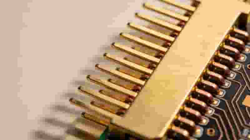
Gold fingers are the gold-plated edge connectors along the side of many PCBs, such as memory cards, graphics cards, SSDs and expansion boards. These flat exposed pads form a plug-in interface that allows the PCB to slide directly into a mating connector or slot without cables.
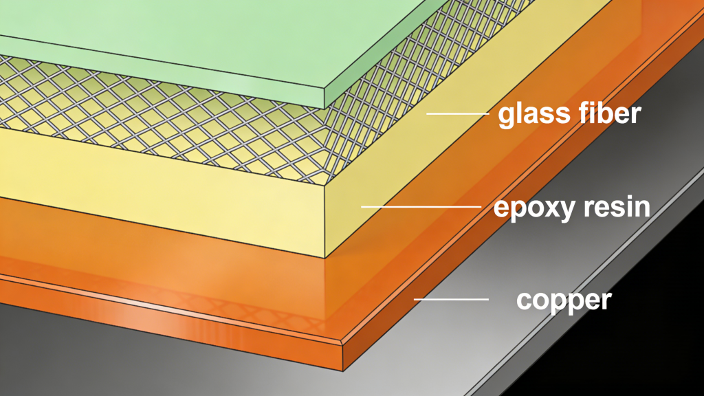
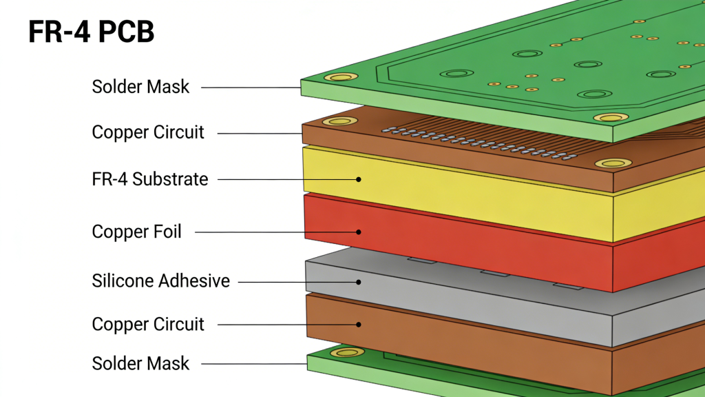
In a Gold Finger PCB, the copper pads at the board edge are covered with hard gold or ENIG surface finish to provide low contact resistance and excellent resistance to oxidation and wear. The fingers are typically beveled at 30°-45° for smooth insertion and reliable contact even after many mating cycles.
By arranging multiple fingers in precise patterns, designers can route power rails, high-speed signals and control lines through a single compact edge connector. This makes Gold Finger PCB ideal for detachable modules, easy upgrades and high-density connections between main boards and daughter cards.
Gold Finger PCB Design Guidelines
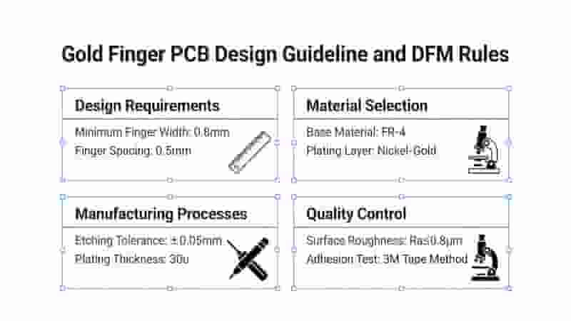
When designing a Gold Finger PCB, geometry and layout rules directly affect reliability, contact resistance and long-term wear performance. Edge connector pads, bevel angle, spacing, surface finish and keep-out areas must be clearly defined.
| Design Parameter | Typical Recommendation | Notes |
|---|---|---|
| Gold Type | Hard Gold or ENIG | Hard gold for frequent mating; ENIG for prototypes |
| Gold Thickness | 3-50 µin hard gold | Thicker for high cycles and harsh environments |
| Bevel Angle | 30°-45° | Smoother insertion and pad protection |
| Finger Width | 0.8-1.5 mm | Match connector footprint and current |
| Solder Mask | No mask on finger pads | Keep contact area fully exposed |
| Vias Near Fingers | 0.5-1.0 mm away | Prevent plating leakage and weakness |
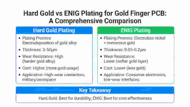
Gold Plating Options & Thickness for Gold Fingers
The surface finish of Gold Finger PCB directly impacts contact resistance, wear life and cost. Most applications use hard electroplated gold or ENIG, based on mating frequency, environment and budget.
| Item | Hard Gold Plating | ENIG |
|---|---|---|
| Plating Method | Electroplated over nickel | Electroless nickel + immersion gold |
| Gold Thickness | 10-50 µin | 1-3 µin |
| Wear Resistance | Very high | Moderate |
| Best For | High-cycle production | Prototypes & low cycles |
We recommend gold thickness based on mating cycles: 3-5 µin for prototypes, 10-20 µin for medium cycles, and 30-50 µin for high-cycle or mission-critical Gold Finger PCB applications.
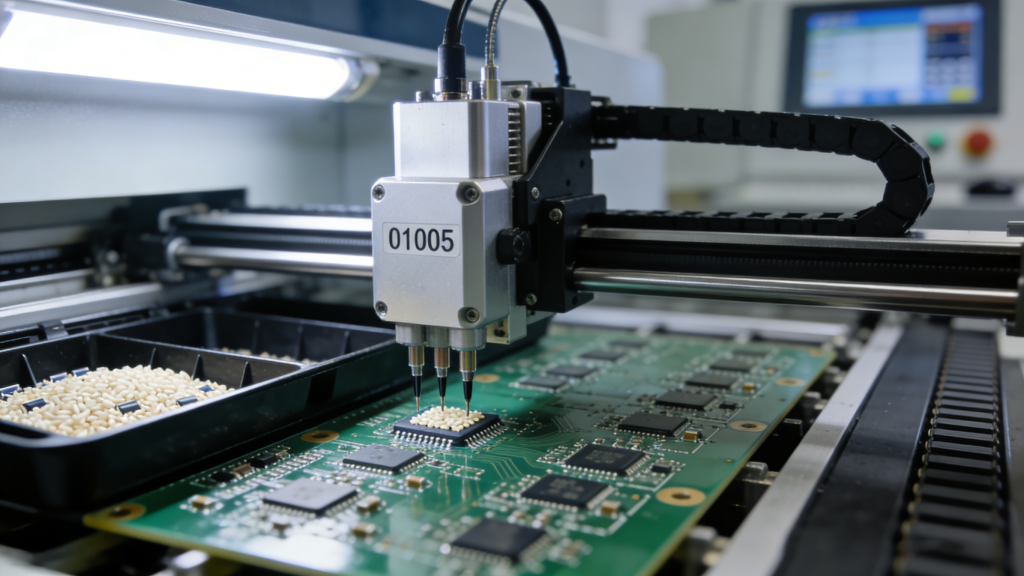
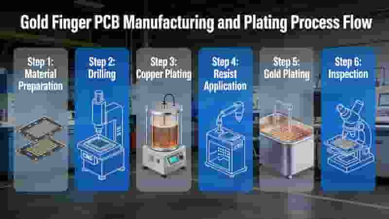
Gold Finger PCB Manufacturing Process
Our Gold Finger PCB production follows strict IPC standards with specialized steps for edge connectors:
- Core PCB fabrication: lamination, etching, drilling, and plating
- Edge connector preparation: clean exposed copper pads
- Nickel underlayer plating as barrier layer
- Gold plating on fingers to target thickness
- Precision beveling at 30°-45°
- Solder mask and silkscreen application (keep fingers clear)
- AOI and electrical testing for 100% quality
Applications of Gold Finger PCBs
Gold Finger PCB provides compact, reliable removable connections widely used in:
- Computing: RAM, GPU, PCIe cards, SSD modules
- Networking: interface cards, optical modules, backplanes
- Industrial: PLC I/O cards, motion control modules
- Consumer: memory adapters, docking stations, game cartridges
- Medical & test: data acquisition, interface boards
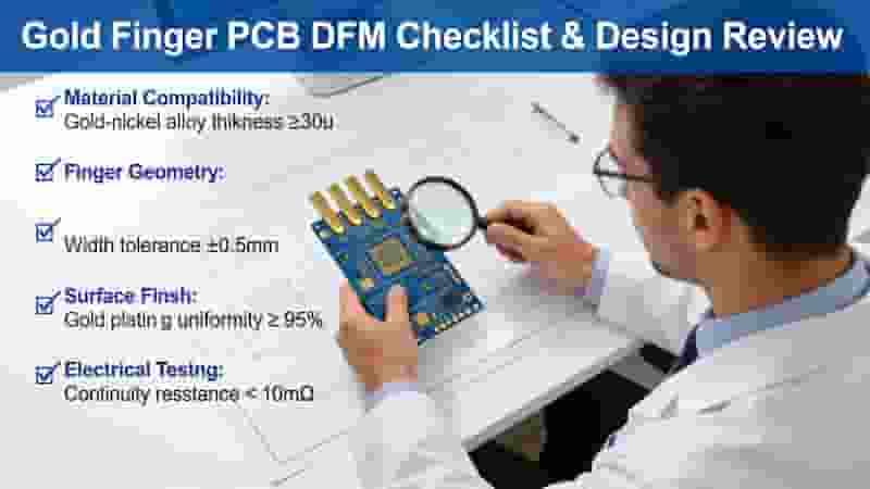
Gold Finger PCB Design Checklist (DFM)
- Confirm connector type, bevel angle, and board thickness
- Define finger count, width, pitch matching connector
- Select hard gold or ENIG and proper thickness
- Keep solder mask and silkscreen away from fingers
- Avoid vias in or near finger pads (0.5-1.0 mm clearance)
- Maintain copper balance and routing at board edge
- Verify stack-up and impedance for high-speed signals
- Add clear fabrication notes for gold fingers
Summary
Gold Finger PCB is a critical component for edge-connector applications requiring stable connection, wear resistance, and long service life. We provide full-cycle manufacturing with hard gold/ENIG plating, precision beveling, IPC compliance, and free DFM review to support your prototype and mass production needs.
Ready to Start Your Gold Finger PCB Project?
Get high-quality Gold Finger PCB with fast lead times, professional engineering support, and competitive pricing. We accept Gerber files, provide free DFM analysis, and deliver reliable boards for global industrial buyers.