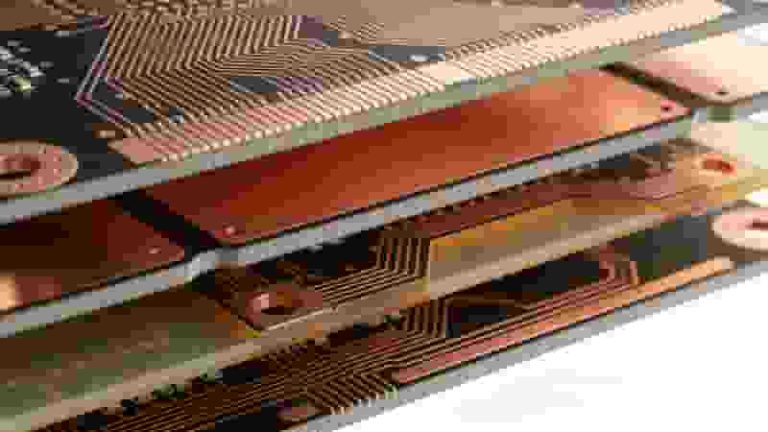
Plated half-holes (also known as castellated holes) offer a space-efficient, reliable method for interconnecting PCB modules through direct soldering. Positioned at board edges, they simplify assembly, improve alignment, and boost mechanical stability compared to traditional bottom pads. This guide covers structure, design rules, fabrication, benefits, applications, and best practices for engineers and buyers.
What Are Plated Half-Holes (Castellated Holes)?
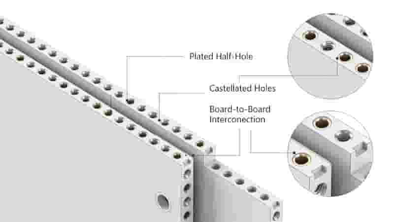
Plated half-holes, or castellated holes, are edge-mounted plated through-holes that provide reliable board-to-board interconnection without connectors. They are partially milled at the PCB edge to form a semi-circular copper pad for direct SMT soldering.
Unlike internal pads, castellated holes improve access during assembly, inspection, and rework, making them ideal for compact, high-density designs.
Structure of Plated Half-Holes
Plated half-holes share structural similarities with plated through-holes but are precisely bisected at the board edge. Only the wall of one side remains copper-plated.
This structure creates a robust, exposed contact surface ideal for soldering modules to motherboards or adjacent boards. It ensures better coaxial alignment and mechanical strength than under-board pads.
Plated Half-Hole Design Guidelines
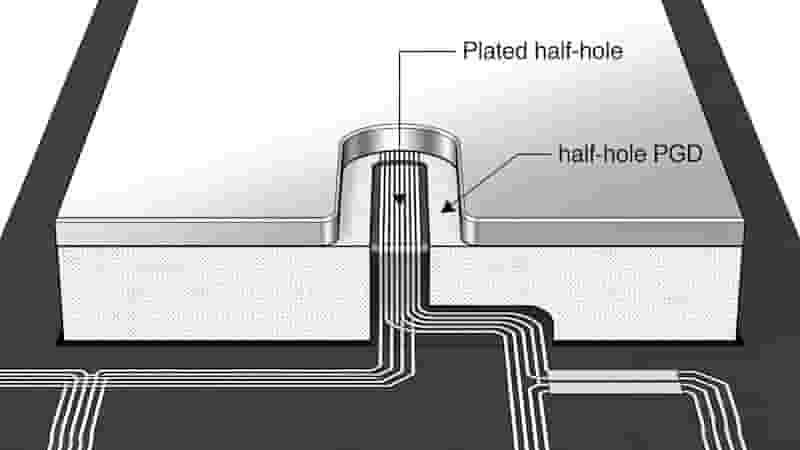
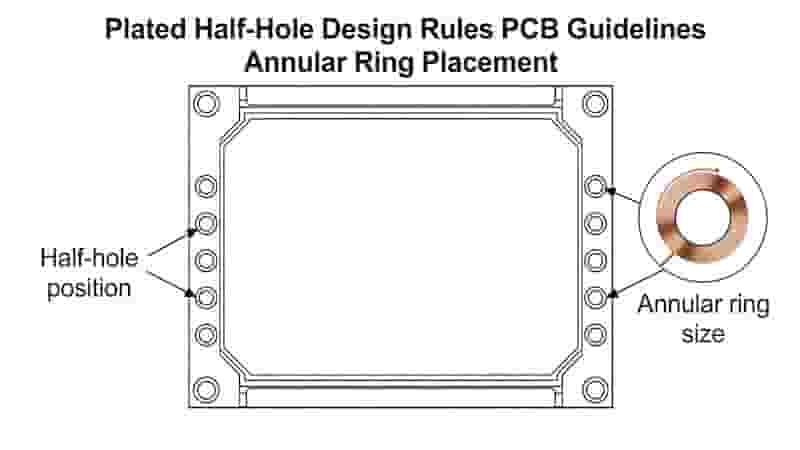
Follow these critical rules to ensure plated half-holes are manufacturable, reliable, and assembly-friendly:
- Place castellated holes precisely at board edges for full access
- Define them as plated through-holes in your EDA software
- Include them clearly in drill and rout files
- Add anti-pad clearance on all inner layers
- Follow minimum diameter and annular ring requirements
- Balance hole size for reliability, routing, and cost

Plated Half-Hole Fabrication Process
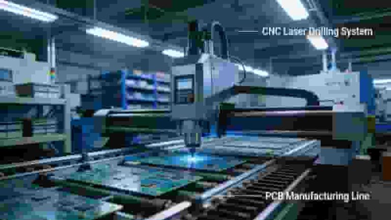
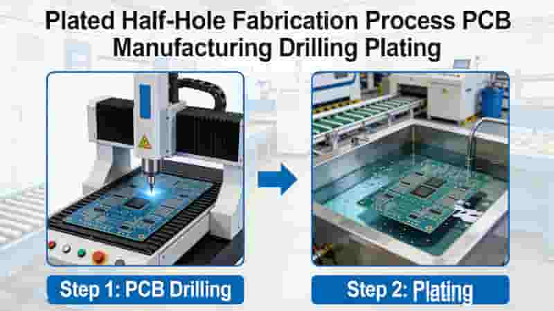
Modern plated half-hole manufacturing uses precision routing or laser cutting after plating to ensure clean copper walls and consistent quality.
Advanced processes avoid burrs, improve plating uniformity, and support mass production. Advanced laser processing delivers higher precision for miniaturized castellated holes.
Key Benefits of Castellated Holes
Plated half-holes deliver clear advantages over conventional connection methods:
- Simplify soldering, inspection, and rework
- Improve coaxial alignment and mechanical stability
- Reduce assembly time and BOM cost
- Avoid dust traps and contamination issues
- Support high-density interconnect and miniaturization
- Enhance reliability in vibration-prone environments
Industrial Applications
Plated half-holes are widely used in modern electronics:
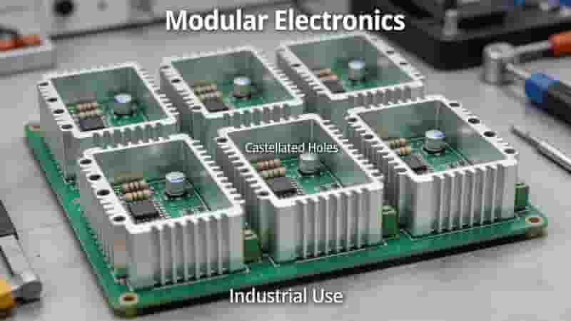
- Modular PCB assemblies
- High-density SMT systems
- Portable and compact devices
- Rigid-flex PCB interconnections
- IoT and industrial control modules
- Automotive and medical sub-assemblies
Conclusion
Plated half-holes (castellated holes) are a proven, cost-effective solution for reliable board-to-board soldering in compact PCB designs. Proper design and fabrication ensure high yield, strong connectivity, and long-term performance.
We specialize in manufacturing high-precision plated half-hole PCBs for global industrial clients, with strict DFM, IPC standards, and full process control.
Need Plated Half-Hole PCB Manufacturing or Quotation?
Contact us for custom design support, DFM review, prototype, and mass production solutions.
Request a Quote Now
What is FR-4 Material in PCB Fabrication? The Complete Engineering Guide
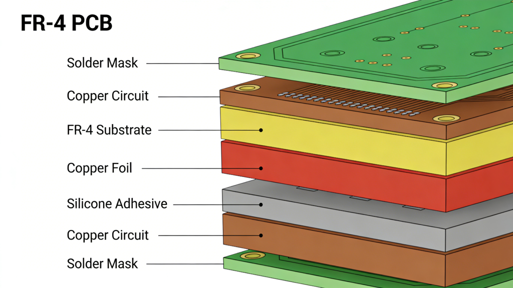
What is FR-4 Material in PCB Fabrication? Complete Engineering Guide
What is a Surface Mount Device or SMD Component Package?
Turnkey PCB Assembly Services | Full & Partial Solutions
Through-hole PCB Assembly Service | IPC Certified THT PCBA Solutions