Discover the differences between single-layer PCB, double-sided PCB, and multilayer PCBs with our expert guide. Learn their applications, advantages, and how to choose the right PCB for your project.
Introduction
Printed Circuit Boards (PCBs) are the foundation of modern electronics, serving as the critical platform that connects and powers components in devices ranging from simple gadgets to sophisticated industrial systems. Whether you’re a hobbyist designing a prototype, an engineer developing a consumer product, or a manufacturer scaling production, choosing the right PCB type is a pivotal decision that impacts performance, cost, and reliability.
At our company, we’ve been empowering global clients with high-quality PCB manufacturing solutions for years, offering everything from single-layer PCB and double-sided PCB to advanced multilayer boards (up to 32 layers) and flexible PCBs. Our expertise ensures that you get the right PCB for your application, whether it’s a cost-effective solution for a simple circuit or a complex design for cutting-edge technology.
What Are Single-Sided and Double-Sided PCBs?
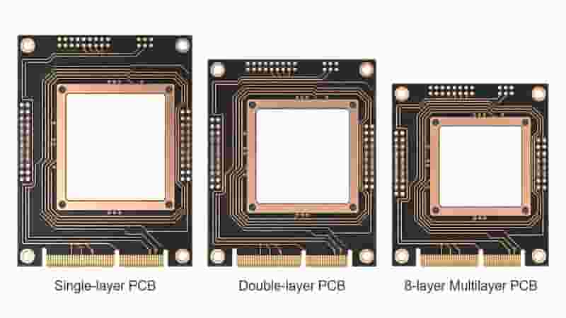
Single-Sided PCBs (Single-layer PCB)
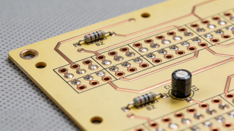
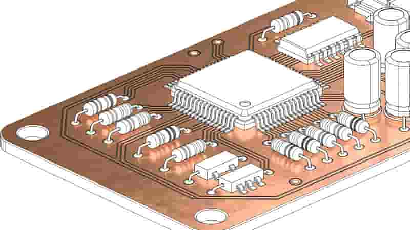
A single-layer PCB consists of a single conductive layer on one side of an insulating substrate, typically FR-4. The conductive layer is made of thin copper foil etched into traces and pads, protected by a solder mask and labeled with a silkscreen layer.
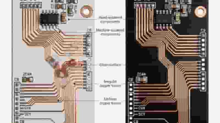
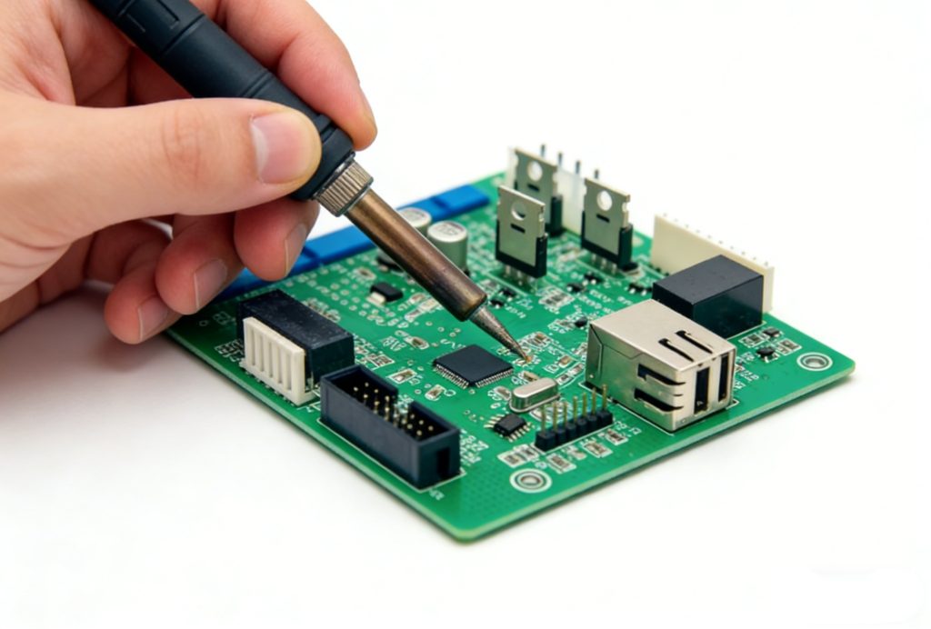
Components are mounted via through-hole technology or surface-mount technology (SMT). Single-layer PCB designs work best for simple circuits with low component density.
Double-Sided PCBs
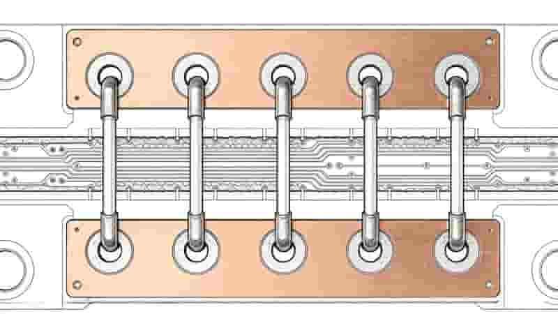
A double-sided PCB has conductive copper layers on both sides of the FR-4 substrate, connected by plated through-holes (vias). This doubles routing space and supports higher component density.
Double-sided PCBs support mixed through-hole and SMT assembly on both sides, making them ideal for compact, complex electronics.
Key Differences Between Single-layer PCB and Double-sided PCB
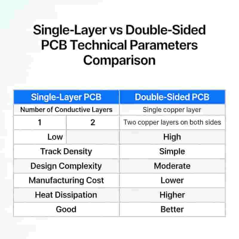
| Feature | Single-layer PCB | Double-sided PCB |
|---|---|---|
| Conductive Layers | 1 layer | 2 layers |
| Vias | None | Plated through-holes |
| Component Density | Low | High |
| Circuit Complexity | Simple | Complex |
| Manufacturing Cost | Lowest | Moderate |
Advantages and Disadvantages
Single-layer PCB Pros & Cons
Advantages:
- Lowest manufacturing cost
- Simplest production process
- High reliability for basic circuits
- Ideal for high-volume, low-cost products
Disadvantages:
- Limited routing space
- Not suitable for complex circuits
- Larger board size for same functionality
Double-sided PCB Pros & Cons
Advantages:
- Double routing space and design flexibility
- Higher component density
- Better signal integrity and EMC performance
- Supports high-speed and compact designs
Disadvantages:
- Higher material and production cost
- More complex manufacturing process
- Longer production lead time
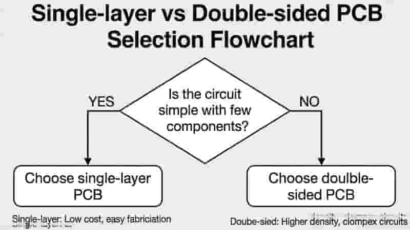
How to Choose Between Single-layer PCB and Double-sided PCB
Choose a single-layer PCB if you need:
- Simple circuits with low component count
- Ultra-low-cost mass production
- Low-frequency applications (<10 MHz)
- LED lighting, adapters, toys, basic controllers
Choose a double-sided PCB if you need:
- Compact size and high component density
- High-speed signals or better EMC performance
- Mixed through-hole and SMT assembly
- Automotive, industrial, medical, IoT devices
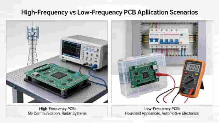
When to Consider Multilayer PCBs
When single-layer PCB and double-sided PCB cannot meet routing, density, or signal integrity needs, multilayer PCBs (3+ layers) become the best choice. They offer dedicated power/ground planes, better EMI shielding, and support for ultra-compact high-speed designs used in 5G, aerospace, and medical equipment.
PCB Design & Manufacturing Best Practices
Optimize trace width per IPC standards, place components strategically to minimize interference, use vias efficiently, and follow DFM rules to reduce costs and errors. Our team provides free DFM review for all single-layer PCB and double-sided PCB orders.
Conclusion
Selecting between single-layer PCB and double-sided PCB depends on your circuit complexity, size constraints, performance needs, and budget. Single-layer PCB delivers the best value for simple, cost-sensitive projects, while double-sided PCB provides flexibility and performance for most modern electronics.
We provide professional single-layer PCB and double-sided PCB manufacturing, assembly, and custom solutions for global industrial buyers and engineers. Our ISO-certified production ensures stable quality, fast delivery, and competitive pricing.
Get Your Custom PCB Quote Today
Request free DFM analysis, instant pricing, and professional PCB manufacturing services for your project.
Request a Free Quote
The Essentials of Microvias – Enabling Miniaturization in PCBs
What is a Pad in PCB Design?
How to Build a Multilayer PCB: Full Stack‑Up, Manufacturing & IPC Compliance Guide
How to Choose the Right Quick Turn PCB Assembly Manufacturer
PCB Terminology Glossary – Over 150 Essential PCB Terms for Engineers & Global Buyers