Learn how to select the ideal PCB surface finish for reliability, solderability, cost, and fine‑pitch assembly. Compare HASL, ENIG, OSP, Immersion Silver, and more for industrial and export projects.
What Is a PCB Surface Finish and Why It Matters
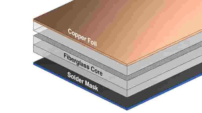
A PCB surface finish is a protective layer applied to exposed copper traces to prevent oxidation, improve solderability, and ensure stable electrical performance. This layer directly affects assembly yield, product lifespan, and cost efficiency for global export projects.
Without a proper surface finish, copper oxidizes rapidly, causing weak solder joints, signal loss, and early failure in industrial, automotive, and consumer electronics.
- Prevents oxidation and corrosion in harsh environments
- Ensures consistent, reliable solder joints during SMT assembly
- Supports fine‑pitch, BGA, and high‑speed PCB designs
- Extends shelf life and storage stability for mass production
Key Factors for Choosing the Right PCB Surface Finish
Selecting the best PCB surface finish requires balancing performance, budget, assembly type, and compliance for international markets.
- Application Environment: Temperature, humidity, and chemical exposure
- Component Type: Fine‑pitch, BGA, QFN, through‑hole, or edge connectors
- Solderability & Assembly Yield: Critical for high‑volume export production
- Shelf Life: Storage time before assembly
- Budget: Low‑cost vs. high‑reliability options
- Compliance: RoHS, IPC, and regional export standards
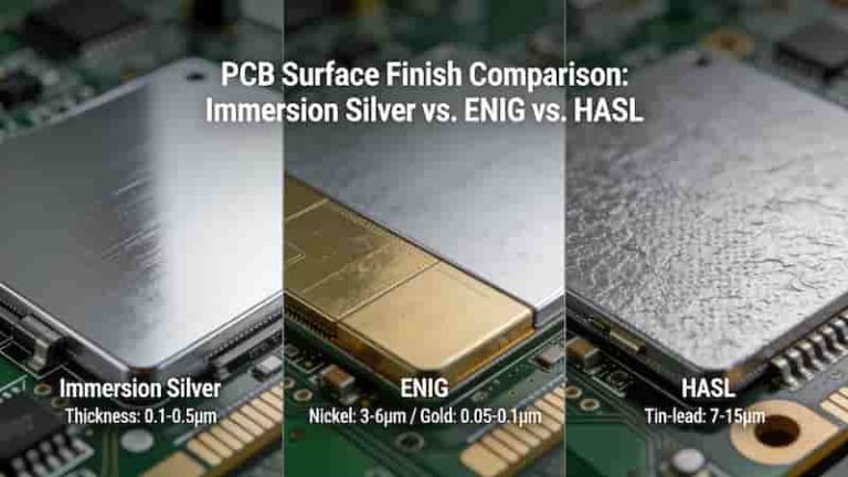
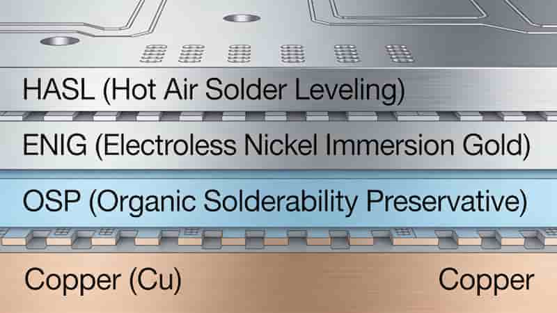
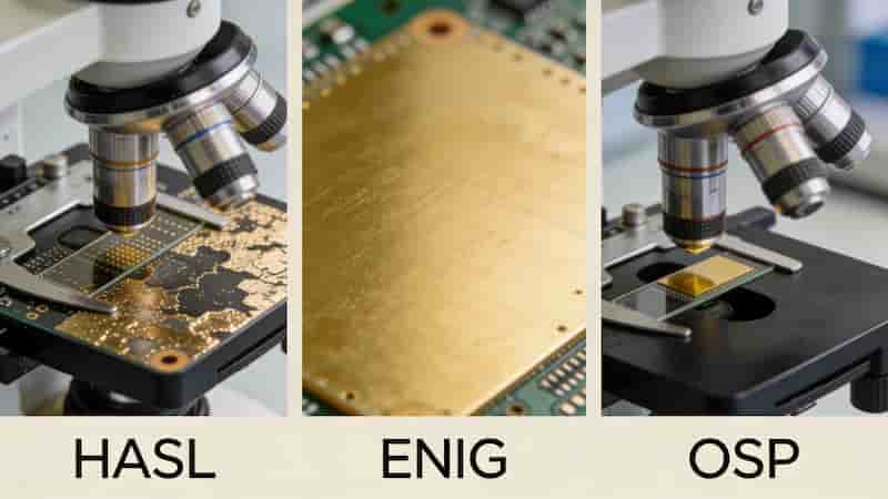
Overview of Common PCB Surface Finishes
Each PCB surface finish provides unique benefits for different industrial applications.
HASL / Lead‑Free HASL
Low‑cost, widely used for general PCBs. Good solderability but poor flatness for fine‑pitch components.
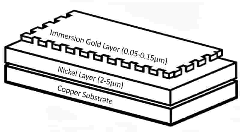
ENIG (Electroless Nickel Immersion Gold)
Premium flat surface, excellent corrosion resistance, ideal for BGA and high‑reliability export products.
OSP (Organic Solderability Preservative)
Eco‑friendly, low‑cost, ultra‑flat surface. Best for high‑volume, fast‑assembly projects.
Immersion Silver & Immersion Tin
Great for high‑speed signals and fine‑pitch; moderate shelf life.
Hard Gold
Durable for edge connectors, test points, and repeated mating.
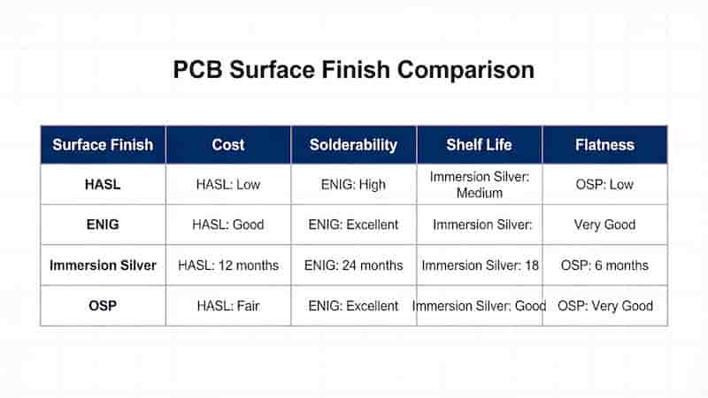
Full Comparison of PCB Surface Finishes
| Finish Type | Cost | Solderability | Shelf Life | Flatness | RoHS | Best For |
|---|---|---|---|---|---|---|
| HASL | Low | Excellent | Long | Poor | No | General PCBs |
| Lead‑Free HASL | Low | Good | Long | Poor | Yes | Standard RoHS Designs |
| ENIG | High | Excellent | Long | Excellent | Yes | Fine‑pitch, BGA, High‑reliability |
| OSP | Low | Good | Short | Excellent | Yes | High‑volume, Fast assembly |
| Immersion Silver | Medium | Excellent | Medium | Excellent | Yes | High‑speed, RF PCBs |
| Hard Gold | High | Poor | Long | Good | Yes | Edge connectors, Test points |
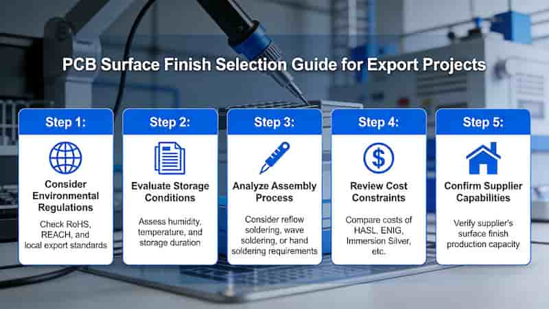
Practical Tips to Choose the Right PCB Surface Finish
Use these professional tips to select the ideal PCB surface finish for export and industrial projects.
- Use ENIG for high‑reliability, fine‑pitch, and long‑term storage
- Choose OSP for low‑cost, high‑volume, and fast assembly
- Select Immersion Silver for high‑speed and RF signal designs
- Use Lead‑Free HASL for general‑purpose RoHS‑compliant boards
- Always confirm compatibility with your assembly process and export standards
Conclusion
Choosing the right PCB surface finish directly impacts performance, reliability, cost, and global market acceptance. Whether you need ENIG for high‑end products, OSP for mass production, or HASL for prototyping, matching the finish to your project requirements ensures stable assembly and long‑term durability.
For industrial export projects, always prioritize PCB surface finish compatibility with assembly, compliance, and environmental conditions.
Optimal PCB Surface Finish for Your Project
Get Expert PCB Surface Finish Support
Need professional advice on PCB surface finish selection, custom manufacturing, or export‑ready PCB production? We provide full engineering support and reliable solutions for global buyers.
Inquire Now | Get Free Quote
Backdrilling of Vias: The Definitive Guide for High-Speed PCB Signal Integrity
PCB Immersion Gold (ENIG) Surface Finish: Full Guide for Reliable Lead-Free PCBs
PCB Vias Explained: Through, Blind, and Buried Vias for Industrial PCB Design
SMT PCB Assembly Services for Prototypes & Production
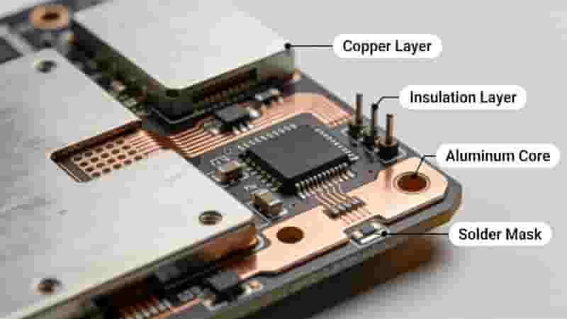
Professional Metal Core PCB (MCPCB) Manufacturing & Custom Service in China